Nano-meta-material full-color-gamut palette

A metamaterial and palette technology, applied in the fields of nanophotonics and ion photonics, can solve the problems of non-adjustable color, affect color fastness, chemical instability of pigment substances, etc., and achieve precise adjustment of color output, color Environmentally friendly, pollution-free, colorful effect

Inactive Publication Date: 2016-01-20
PEKING UNIV
View PDF2 Cites 15 Cited by
  • Summary
  • Abstract
  • Description
  • Claims
  • Application Information

AI Technical Summary

Problems solved by technology

Traditional color production is based on pigments, but there are still several obvious problems: (1) The color purity obtained by toning is not high enough; (2) The pigment substance is chemically unstable, and it is easy to cause fading and decolorization under long-term strong light exposure. Affect the color fastness; (3) The color of the pigment is sensitive to the ambient humidity and temperature, which is easy to cause the change of the color tone and affect the durability of the color; (4) Most of the pigments contain lead, arsenic, chromium, antimony, cadmium, mercury, etc. Substances, the pigment volatilizes or cracks under strong light to produce toxic substances, which brings great harm to the human body and the environment
However, the current plasma color still has certain limitations: (1) color non-adjustability: only a single pixel can achieve a single color; (2) limited color types: color mixing is achieved by combining pixels, but due to processing technology means Limitations, the types of structural colors dependent on the structure size are limited; (3) The pixel size is difficult to reduce: the plasmonic color based on the metal-dielectric-metal structure mostly depends on the periodic arrangement of the structure, and the repetitive arrangement of the structure limits the pixel size. make it difficult to shrink further

Method used


Image

  • Nano-meta-material full-color-gamut palette
  • Nano-meta-material full-color-gamut palette
  • Nano-meta-material full-color-gamut palette

Examples


Embodiment 1

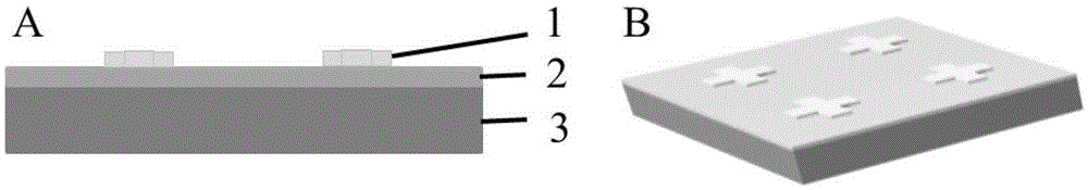
[0024] (1) thermal oxidation passivation layer: utilize thermal oxidation growth on the surface of silicon (Si) substrate 1 Thick SiO 2 as a passivation layer.

[0025] (2) Photolithography patterning: in Si / SiO 2AR-N7520.18 negative photoresist with a thickness of 100nm was spin-coated on the surface at a speed of 5000 revolutions per second, pre-baked in an oven at 85°C for 5 minutes, and the photoresist was subjected to an acceleration voltage of 80kV using a NanoBeam electron beam etching system. Expose, develop in tetramethylammonium hydroxide (TMAH) developing solution for 1 minute and rinse with deionized water to obtain an imaged nanostructure array;

[0026] (3) Dielectric layer formation: use silicon oxide as a mask, etch the silicon substrate with a reactive ion etching machine, the power of the etching machine is 400W, SF 6 and C 4 f 8 The flow rates were 40 and 90 sccm / min, respectively, and the etching time was 50 seconds. Due to the scallop effect of the e...

Embodiment 2

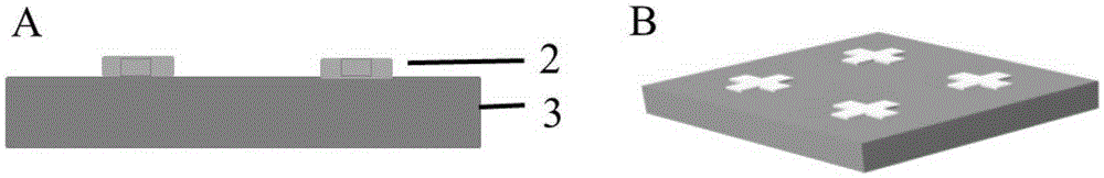
[0029] (1) Chemical vapor deposition mask layer: grown on the surface of silicon (Si) substrate by chemical vapor deposition (CVD) Thick SiO 2 as a mask layer.

[0030] (2) Photolithography patterning: in Si / SiO 2 AR-N7520.18 negative photoresist with a thickness of 100nm was spin-coated on the surface at a speed of 5000 revolutions per second, pre-baked in an oven at 85°C for 5 minutes, and the photoresist was subjected to an acceleration voltage of 80kV using a NanoBeam electron beam etching system. Expose, develop in tetramethylammonium hydroxide (TMAH) developing solution for 1 minute and rinse with deionized water to obtain an imaged nanostructure array;

[0031] (3) Dielectric layer formation: use photoresist and silicon oxide as a mask, and use a reactive ion etching machine to perform isotropic etching on the silicon substrate. The power of the etching machine is 400W, SF 6 and C 4 f 8 The flow rates are 40 and 90 sccm / min respectively, and the etching time is 50...

Embodiment 3

[0035] (1) Photolithographic patterning: Spin-coat AR-N7520.18 negative photoresist with a thickness of 100nm on the surface of the glass substrate at a speed of 5000 revolutions per second, pre-bake in an oven at 85°C for 5 minutes, and use NanoBeam The electron beam etching system exposes the photoresist with an accelerating voltage of 80kV, develops it in tetramethylammonium hydroxide (TMAH) developer solution for 1 minute, and rinses it with deionized water to obtain an imaged nanostructure array;

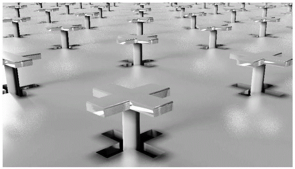
[0036] (2) Dielectric layer formation: using photoresist as a mask, use a reactive ion etching machine to etch the glass substrate isotropically, the power of the etching machine is 400W, SF 6 and C 4 f 8 The flow rates are 40 and 90 sccm / min, respectively, and the etching time is 50 seconds to form nanopillars with a height of 100nm and the suspended silicon nanostructure array supported by them;

[0037] (3) Metal-medium-metal three-dimensional structure: a 30nm gold nanola...


PUM


Abstract

The invention discloses a nano-meta-material full-color-gamut palette and a preparation method thereof. Electron beam photo-etching and reactive ion etching technologies are adopted; a transverse undercutting effect is utilized for obtaining a sub-wavelength periodic-structure array, which suspends above a dielectric layer, on a substrate; a metal film is deposited in the direction perpendicular to the substrate; and forming a metal nanostructured array-metal complementation nanostructured array film coupled structure. The sub-wavelength meta-material shows a mixed surface plasma resonance mode in a visible light spectrum and generates specific optical responses such as multiple resonance peaks, FANO resonance, angle-dependent spectrum adjustability and hundreds of thousands of times field enhancement, so that continuous and adjustable colors can be obtained in a structural unit. The nano-meta-material palette can generate full-color-gamut colors in a CIE chromaticity diagram, and the color pixel can be reduced to one hundred to hundreds of nanometers. The technology provided by the invention has an important application prospect in the fields such as product production, high-definition displaying, artistic creation, orientation sensing, photon codes and information storage.

Description

technical field [0001] The present invention relates to nano-processing and manufacturing technology, surface plasmon photonics, and nano-photonics, and in particular to a palette of nano-metamaterials based on surface plasmon coupling effects. Its technical characteristics: (1) Nano-antenna structure surface plasmon Body coupling, the reflection or extinction spectrum of the coupled structure has multiple resonance peaks in the visible region; (2) The shape and period of the metamaterial structure can be controlled to produce different resonance peaks; (3) The resonance coupling of the nano-antenna is realized in a pixel unit Reconcile a variety of spectral colors, similar to the function of an artist's palette; (4) The color development of the metamaterial palette is sensitive to the incident angle and intensity, and can be stimulated to produce rich colors, including the spectral colors in the CIE chromaticity diagram , non-spectral colors, and continuously adjustable inter...

Claims


Application Information

Patent Timeline
Patent Type & Authority Applications(China)
IPC IPC(8): G02B5/00
CPCG02B5/008
Inventor 吴文刚樊姣荣朱佳谌灼杰毛逸飞
Owner PEKING UNIV
Why Eureka
Try Eureka