Up-conversion luminescent structure capable of raising luminescence intensity and preparation method
A technology of luminescent structure and luminous intensity, applied in luminescent materials, chemical instruments and methods, photovoltaic power generation, etc., can solve problems such as unseen KLaF films, achieve regulation and enhancement, solve low luminous intensity, and simple preparation process. Effect
- Summary
- Abstract
- Description
- Claims
- Application Information
AI Technical Summary
Problems solved by technology
Method used
Image
Examples
Embodiment 1
[0028] Embodiment 1 Ag thin film / lanthanum potassium fluoride thin film light-emitting structure without ZnO dielectric layer
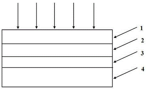
[0029] (1) Weigh 50 mg of polymethyl methacrylate (PMMA) powder and place it in a stirring bottle, then add 4 mL of chloroform solvent, stir for 30 minutes, then add 30~50 mg of aluminum-doped KLaF 4 : Yb 3+ / Er 3+ powder, continue to stir for 24 hours to obtain a transparent colloidal solution;
[0030] (2) Clean the common glass substrate and dry it;
[0031] (3) Deposit a metal Ag film on the glass substrate by vacuum evaporation method, with a thickness of about 10-20nm;
[0032] (4) Spin-coat the colloidal solution obtained in step (1) on the Ag film. The spin-coating conditions are: forward rotation speed 650rmp, time 12s; back rotation speed 2000rmp, time 30s;
[0033] (5) After the film is dry, repeat the step (4) to obtain an up-conversion light-emitting layer with a thickness of 50-100 nm.
Embodiment 2
[0034] Example 2 Ag thin film / lanthanum potassium fluoride thin film light emitting structure containing ZnO dielectric layer
[0035] (1) Weigh 50 mg of polymethyl methacrylate (PMMA) powder and place it in a stirring bottle, then add 4 mL of chloroform solvent, stir for 30 minutes, then add 30~50 mg of aluminum-doped KLaF 4 : Yb 3+ / Er 3+ powder, continue to stir for 24 hours to obtain a transparent colloidal solution;
[0036] (2) Clean the common glass substrate and dry it;
[0037] (3) Deposit a metal Ag film on the glass substrate by vacuum evaporation method, with a thickness of about 10-20nm;
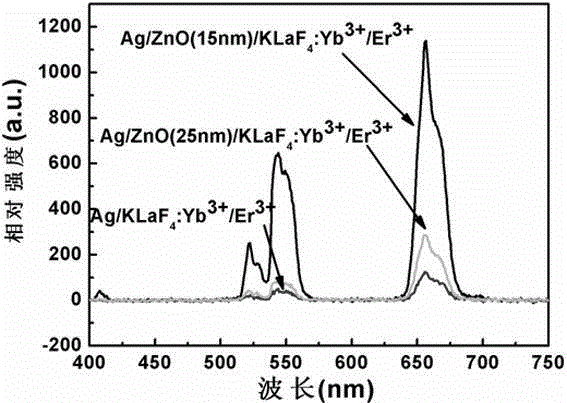
[0038] (4) Deposit zinc oxide on the metal Ag film by radio frequency magnetron sputtering. The sputtering process conditions are: use zinc oxide ceramic target, and the background vacuum is less than 6×10 -4 Pa, target base distance 75mm, Ar gas flow rate 60sccm, sputtering pressure 0.5Pa, sputtering power 100W, the zinc oxide film thickness obtained is 5~25nm;
[0039] ...
Embodiment 3
[0042] Example 3 Light-emitting structure of Au thin film / lanthanum potassium fluoride thin film without ZnO dielectric layer
[0043] (1) Weigh 50 mg of polymethyl methacrylate (PMMA) powder and place it in a stirring bottle, then add 4 mL of chloroform solvent, stir for 30 minutes, then add 30~50 mg of aluminum-doped KLaF 4 : Yb 3+ / Er 3+powder, continue to stir for 24 hours to obtain a transparent colloidal solution;
[0044] (2) Clean the common glass substrate and dry it;
[0045] (3) Deposit metal Au film on the glass substrate by vacuum evaporation method, the thickness is about 10~20nm;
[0046] (4) Spin-coat the colloidal solution obtained in step (1) on the Au film. The spin-coating conditions are: forward rotation speed 650rmp, time 12s; back rotation speed 2000rmp, time 30s;
[0047] (5) After the film is dry, repeat the step (4) to obtain an up-conversion light-emitting layer with a thickness of 50-100 nm.
PUM
| Property | Measurement | Unit |
|---|---|---|
| Thickness | aaaaa | aaaaa |
Abstract
Description
Claims
Application Information


