Method for preparing organic field effect transistor dielectric layer by using plasma crosslinking technology
A plasma and dielectric layer technology, which is applied in semiconductor/solid-state device manufacturing, circuits, electrical components, etc., can solve the problems that cannot meet the needs of flexible devices, large leakage current of devices, etc., to overcome inflexibility and improve the surface The effect of simple features and equipment
- Summary
- Abstract
- Description
- Claims
- Application Information
AI Technical Summary
Problems solved by technology
Method used
Image


Examples
Embodiment 1
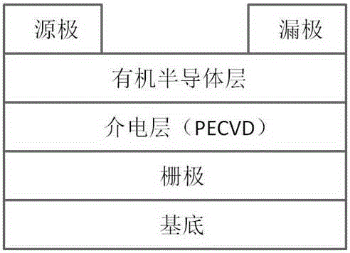
[0024] A preparation of an organic field effect transistor, the organic field effect transistor includes a substrate, a gate electrode, a dielectric layer (PECVD), an organic semiconductor layer, and source and drain electrodes;
[0025] Specific steps:
[0026] Step 1: Cleaning the Silicon Substrate
[0027] The n-type heavily doped silicon substrate without silicon dioxide was cleaned sequentially with detergent, tap water, deionized water, acetone, and absolute ethanol for 10 minutes, and then dried with nitrogen.
[0028] The second step, plasma-enhanced chemical vapor deposition to prepare the cross-linked dielectric layer
[0029] The semi-finished product prepared above is placed in a vacuum chamber, and a mixed gas of argon and acetylene is introduced at a ratio of 5:3, and the pressure is maintained at 10Pa. The plasma is generated by inductively coupled discharge, the power is 100W, and the processing time is 30 minutes. An ultra-thin dielectric layer is formed to ...
Embodiment 2
[0035] A preparation of an organic field effect transistor, the organic field effect transistor includes a substrate, a gate electrode, an insulating layer, a dielectric layer (PECVD), an organic semiconductor layer, and source and drain electrodes, such as figure 1 shown.
[0036] Specific steps:
[0037] Step 1: Cleaning the Silicon Substrate
[0038] The n-type heavily doped silicon substrate without silicon dioxide was cleaned sequentially with detergent, tap water, deionized water, acetone, and absolute ethanol for 10 minutes, and then dried with nitrogen.
[0039] Step 2: Preparation of insulating layer by solution method
[0040] A polyvinyl alcohol solution with a mass fraction of 8wt% was prepared, the solution was coated on a silicon substrate, and a dielectric layer was prepared by spin coating at a rotational speed of about 2000rpm, and then dried to a thickness of about 800nm.
[0041] The third step, plasma-enhanced chemical vapor deposition to prepare the cro...
PUM
| Property | Measurement | Unit |
|---|---|---|
| Thickness | aaaaa | aaaaa |
Abstract
Description
Claims
Application Information
PatSnap Eureka turns technology decisions into work you can execute. Powered by our Innovation Knowledge Graph, it runs expert workflows across engineering, life sciences, materials and intellectual property. Get your review-ready output in minutes.


