
A kind of fully fluorescent white light organic light-emitting diode and its preparation method

A light-emitting diode and all-fluorescence technology, which is applied in the manufacture of semiconductor/solid-state devices, electrical components, and electric solid-state devices, can solve the problems of unsatisfactory quantum efficiency and color rendering index, poor performance, etc., and achieve reduced material costs and high luminescence Efficiency, to achieve the effect of luminous efficiency

Active Publication Date: 2018-01-05
SOUTH CHINA UNIV OF TECH
View PDF5 Cites 0 Cited by
  • Summary
  • Abstract
  • Description
  • Claims
  • Application Information

AI Technical Summary

Problems solved by technology

However, its poor performance must be significantly improved before the preparation of white OLED devices to meet the requirements of realizing high-efficiency all-fluorescent white OLED devices.
In view of the unsatisfactory external quantum efficiency and color rendering index of all fluorescent white organic light-emitting diode devices, it is urgent to find a new device design idea, based on the new device structure to achieve high efficiency using traditional fluorescent organic materials as dopants Fully fluorescent white organic light-emitting diode devices with high efficiency and high color rendering index

Method used


Image

  • A kind of fully fluorescent white light organic light-emitting diode and its preparation method
  • A kind of fully fluorescent white light organic light-emitting diode and its preparation method
  • A kind of fully fluorescent white light organic light-emitting diode and its preparation method

Examples


Embodiment 1

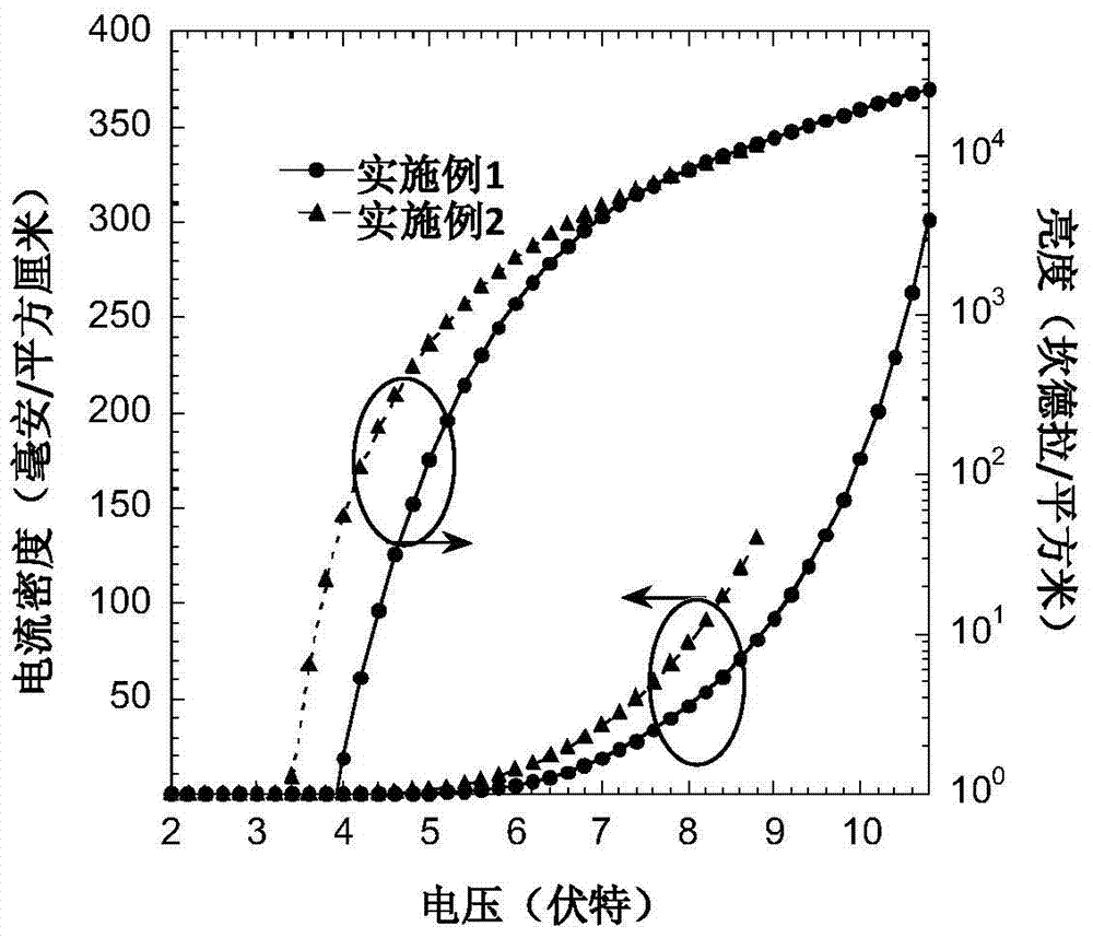
[0035] Take a number of ITO conductive glass substrates with the same batch number, the size is 30 mm × 30 mm, the thickness of ITO is about 90 nanometers, and its square resistance is about 20 ohms / square. Sequentially use acetone, special detergent for micron semiconductors, deionized water, and isopropanol to ultrasonically clean for 15 minutes to remove dirt on the surface of the substrate. Then put it into an incubator to dry at 80 degrees Celsius. The dried ITO substrate was treated with a plasma (plasma) ignition device for 4 minutes to further remove organic impurities attached to the surface. Then the ITO substrate was transferred to a glove box filled with high-purity nitrogen gas without water and oxygen. In this glove box, the devices are loaded into the vacuum plating chamber. Turn on the mechanical pump and molecular pump, when the vacuum in the plating chamber is less than 5×10 -4 The thermal evaporation film starts after Pa. Using a specific mask, sequentia...

Embodiment 2

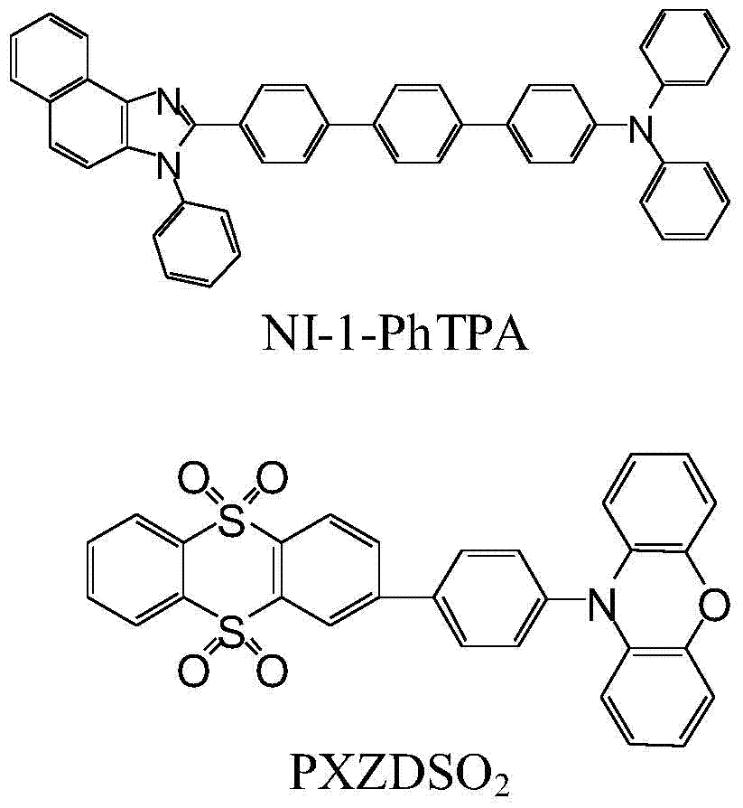
[0042] The preparation process was the same as in Example 1, and the anode buffer layer material HAT-CN, the hole transport layer material TAPC, the blend of the deep blue fluorescent light-emitting layer material CBP and 10wt% NI-1-PhTPA were evaporated sequentially (CBP: 10wt% NI- 1-PhTPA), intermediate layer material CBP, and blue light to form a complementary color light-emitting layer material is CBP and 5wt% PXZDSO 2 and 0.35 wt% DBP(5,10,15,20-tetraphenylbisbenzo[5,6]indeno[1,2,3-CD:1',2',3'-LM], dibenzo{ Blend of [f,f']-4,4',7,7'-tetraphenyl}diindeno[1,2,3-cd:1',2',3'-lm]perylene) (CBP:5wt% BYZGR 2: 0.35wt% DBP), intermediate layer material CBP, dark blue fluorescent light emitting layer is a blend material CBP: 10wt% NI-1-PhTPA, electron transport layer material TmPyPB, cathode buffer layer material lithium fluoride, cathode material metal aluminum. The evaporation rate and thickness of each functional layer to be evaporated are monitored in real time by a quartz cry...


PUM


Abstract

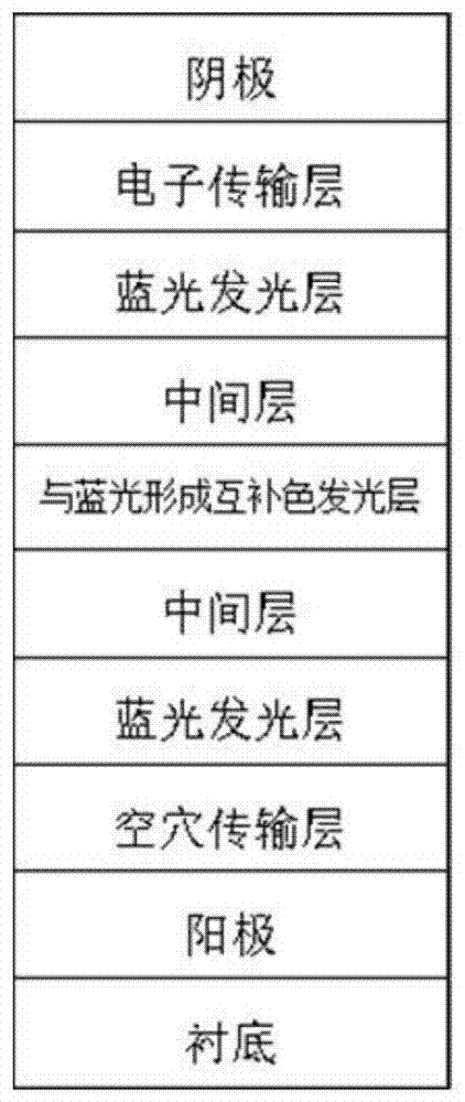
The invention belongs to the technical field of organic photoelectric devices, and discloses a fully fluorescent white light organic light emitting diode and a preparation method thereof. The light emitting diode comprises a substrate, an anode, a hole transport layer, a blue light emitting layer, an intermediate layer, a light emitting layer forming a complementary color with blue light, an intermediate layer, a blue light emitting layer, an electron transport layer and a cathode stacked in sequence. Each corresponding functional layer is realized by an organic semiconductor material capable of serving the corresponding function. The electroluminescent spectrum of the all-fluorescent white organic light-emitting diode of the present invention is derived from fluorescent materials that do not contain precious metals, has low processing costs, high luminous efficiency and high color rendering index, and the theoretical internal quantum efficiency can reach 100%. , has a good application prospect.

Description

technical field [0001] The invention belongs to the technical field of organic photoelectric devices, and in particular relates to an all-fluorescence white light organic light-emitting diode and a preparation method thereof. Background technique [0002] In the 1960s, organic electroluminescence was first observed by applying a bias voltage to single crystal anthracene. The large-scale research and development of organic light-emitting diode devices in the world began in the late 1980s. In 1987, Dr. Deng Qingyun of Kodak Company of the United States invented a sandwich-type organic double-layer thin-film electroluminescent device (patent US4356429), marking that organic electroluminescent technology has entered the era of breeding and practicality. They originally constructed a hole-transporting layer TPD (N,N'-diphenyl-N,N'bis(3-methphenyl)1,1'-biphenyl-4,4'-diamine) and an electron-transporting layer Alq 3 (tris(8-hyroxyquinolinato)aluminum) double-layer device structur...

Claims


Application Information

Patent Timeline
Patent Type & Authority Patents(China)
IPC IPC(8): H01L51/50H01L51/52H01L51/54H01L51/56
CPCH10K30/865H10K50/00H10K50/11H10K50/80H10K71/00
Inventor 苏仕健李祥龙陈东成彭俊彪曹镛
Owner SOUTH CHINA UNIV OF TECH
Learn More