Grating preparation method through pattern transfer based on nano-imprint

A pattern transfer and nano-imprint technology, applied in diffraction grating, patterned surface photoengraving process, optics, etc., can solve the problems of complex process, uncertainty of microstructure pattern, high preparation cost, and achieve optimized preparation process, The effect of easy industrial production and simple preparation method

Inactive Publication Date: 2016-04-13
WUHAN UNIV OF TECH
View PDF3 Cites 19 Cited by
  • Summary
  • Abstract
  • Description
  • Claims
  • Application Information

AI Technical Summary

Problems solved by technology

Due to the complexity of the process, the high cost of preparation and the uncertainty of the microstructure pattern transferred to the...

Method used


Image

  • Grating preparation method through pattern transfer based on nano-imprint
  • Grating preparation method through pattern transfer based on nano-imprint

Examples


Embodiment 1

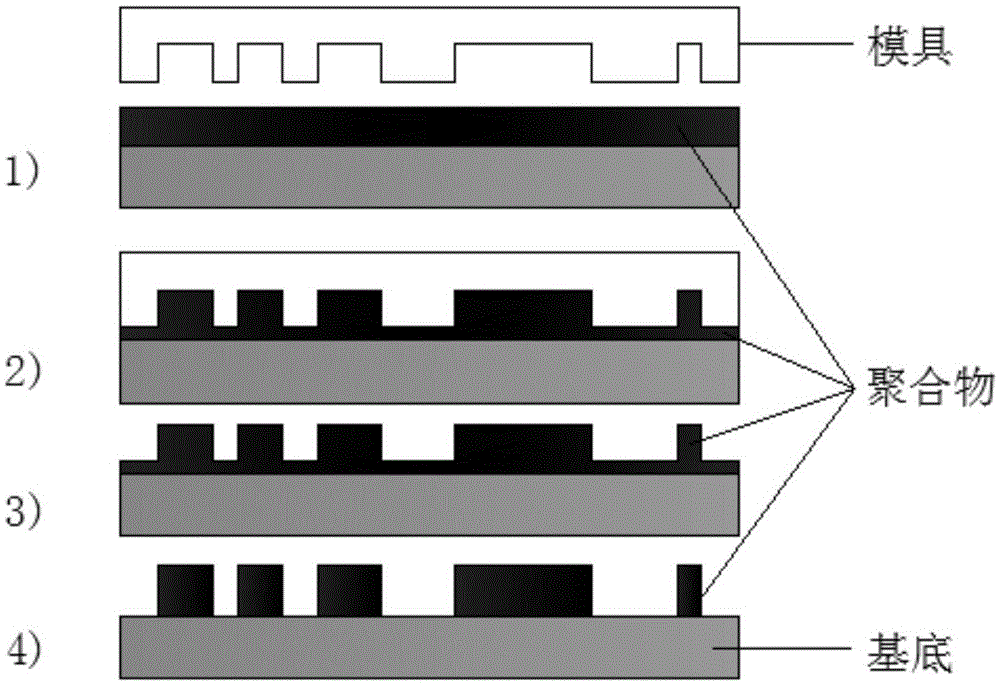
[0026] Step 1): Take a substrate with a clean and smooth upper surface as the substrate for spin-coating polymer photoresist. The material of the substrate can be K9 glass or fused silica, and the shape of the substrate can be round or square. In this embodiment, a circular K9 glass with a diameter of 30mm is used as the substrate, and the pre-coated polymer surface is carefully wiped three times with acetone. After the acetone is naturally volatilized and dried, it is placed in the center of a CT62 plastic rejection table from KarlSuss, Germany. Turn on the hydraulic nitrogen to suck the substrate on the platform, drop 3 drops of polymer (PMMA) solvent into the center of the substrate, set the rotation speed to 3500r / min, and the time to 30s. The thickness of the polymer film spin-coated under this setting is about 350nm . Close the rotary cover and turn on the rotary table. After the gluing is finished, take out the substrate, put it into the oven of Heraeus Company in Germ...

Embodiment 2

[0031] Step 1): Take a round fused silica with a clean and smooth upper surface and a diameter of 30mm as the substrate, carefully wipe the pre-coated polymer surface with acetone three times, and after the acetone evaporates and dries naturally, put it into a CT62 type thrower from KarlSuss Company, Germany. Rubber table center. Turn on the hydraulic nitrogen to suck the substrate on the platform, drop 3 drops of polymer (PS) solvent into the center of the substrate, set the rotation speed to 3000r / min, and the time to 30s. The thickness of the polymer film spin-coated under this setting is about 400nm . Close the rotary cover and turn on the rotary table. After the gluing is finished, take out the substrate, put it into the oven of Heraeus Company in Germany for drying, set the oven temperature to 90°C, and bake for 30 minutes. Quartz substrate.

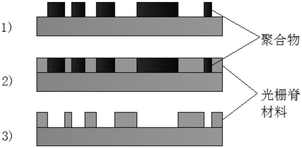
[0032] Step 2): Select a rectangular silicon nitride with a clean and smooth surface of 10mmx10mm as the stamper template mate...


PUM

PropertyMeasurementUnit
Spin coating thicknessaaaaaaaaaa
Thicknessaaaaaaaaaa
Thicknessaaaaaaaaaa

Abstract

The invention belongs to the technical field of optical thin-film micro-nano structures, and provides a grating preparation method through pattern transfer based on nano-imprint. The grating preparation method through pattern transfer based on nano-imprint is characterized by comprising the following steps that 1) polymers are coated on a substrate; 2) a pressing mould template is prepared; 3) the imprint process is performed: the substrate on which the polymers are coated and the pressing mould template are installed on the two imprint discs of an imprint machine, and pressurization is performed when temperature is close to polymer glassy phase change point temperature through heating so that the polymers are enabled to be fully filled with pressing mould patterns and then cooling is performed; and the pressing mould template and the substrate are separated when temperature is close to the phase change point through cooling so that a polymer mask film slot profile is obtained; and 4) micro-nano pattern transfer is performed: required grating ridge material fills in the polymer mask film slot profile by directly using an electron beam evaporation method, deposition thickness is monitored by utilizing the film thickness optical control technology, and then grating structures complementary with the mask film are formed by dissolving the polymer patterns through an organic solvent so that the gratings prepared through pattern transfer based on nano-imprint are obtained. The method is simple in the preparation technology and low in production cost.

Description

technical field [0001] The invention belongs to the technical field of preparation of optical film micro-nano structures, and in particular relates to a method for preparing a grating based on a new micro-nano pattern transfer by nano-imprinting. Background technique [0002] A grating is an optical device composed of a large number of parallel slits of equal width and equal spacing. As a light-splitting element, it is widely used in the fields of spectral measurement, optical calculation, and optical information processing. It is not only a necessary instrument for analyzing the composition of matter and exploring the mysteries of the universe, but also promotes the coordinated development of physics, astronomy, biology and other disciplines. Since Fraunhofer made the world's first grating in 1819, grating manufacturing technology has undergone several major improvements, and each major improvement relies on technological progress and theoretical breakthroughs. Today's grat...

Claims


Application Information

Patent Timeline
IPC IPC(8): G02B5/18G03F7/00
CPCG02B5/1847G03F7/0017
Inventor 夏志林邱志方
Owner WUHAN UNIV OF TECH
Why Eureka
Try Eureka