PERC solar cell and preparation method thereof
A technology of solar cells and permanganate, applied in the field of solar cells, can solve problems such as low yield rate of PERC solar cell products, waste of raw materials, unfavorable applications, etc., to increase open circuit voltage, increase product yield, and reduce junction area recombination Effect
- Summary
- Abstract
- Description
- Claims
- Application Information
AI Technical Summary
Problems solved by technology
Method used
Image
Examples
preparation example Construction
[0025] The preparation method of the PERC solar cell of an embodiment, comprises the steps:
[0026] Carry out double-sided polishing, texturing, diffusion, etching, impurity-removing glass, and permanganate oxidation on silicon wafers in sequence;
[0027] Deposit passivation layer and protective layer on the back;
[0028] Anti-reflective layer deposited on the front;
[0029] Partially opening the back, printing the metal paste on the front and the back, and sintering to obtain a PERC solar cell.
[0030] Among them, the silicon wafer is preferably P-type polysilicon, that is, the method for preparing the PERC solar cell of the present invention is suitable for solar cells made of P-type polysilicon wafers.
[0031] In the double-sided polishing step, it is preferable to use an inorganic alkali solution for double-sided polishing. For example, sodium hydroxide solution is used, but not limited thereto, other inorganic alkali solutions can also be used. The single-side p...
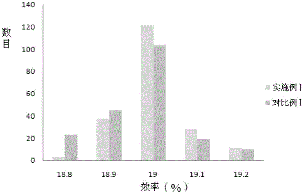
Embodiment 1
[0044] Polish the P-type polysilicon wafer on both sides in a sodium hydroxide solution for 5 minutes. At this time, the thickness reduction after polishing on one side is 10 μm;
[0045] Texturing the above-mentioned polished P-type polysilicon wafers by plasma etching;
[0046] Diffusion of the P-type polysilicon wafer after the above-mentioned texture is carried out by the spin coating method, and the diffusion square resistance is 80ohm / sq;
[0047] Perform Rena removal of the back electrode on the diffused P-type polysilicon wafer;
[0048] Put the above-mentioned P-type polycrystalline silicon chip after removing the back electrode into a permanganic acid solution with a volume fraction of 70%, and maintain it at 75°C for 15 minutes to obtain an oxidized P-type polycrystalline silicon chip;
[0049]On the back of the oxidized P-type polysilicon wafer, deposit an aluminum oxide layer and a silicon nitride film in sequence, and deposit a silicon nitride anti-reflection fi...
PUM
| Property | Measurement | Unit |
|---|---|---|
| Thickness | aaaaa | aaaaa |
| Thickness | aaaaa | aaaaa |
Abstract
Description
Claims
Application Information
