Method for preparing nano-scale graphene structure

A nanoscale, graphene technology, applied in nanotechnology, microlithography exposure equipment, semiconductor/solid-state device manufacturing, etc., can solve problems such as difficult to remove, unreachable, and affect the performance of graphene devices, so as to avoid direct contact, The effect of eliminating influence

Active Publication Date: 2016-06-15
INST OF PHYSICS - CHINESE ACAD OF SCI
View PDF6 Cites 6 Cited by
  • Summary
  • Abstract
  • Description
  • Claims
  • Application Information

AI Technical Summary

Problems solved by technology

However, electron beam lithography technology can achieve precise control and a certain degree of repeatability. The limit size is above 20nm, and cannot reach below 10nm.
In addition, the electron beam

Method used


Image

  • Method for preparing nano-scale graphene structure
  • Method for preparing nano-scale graphene structure
  • Method for preparing nano-scale graphene structure

Examples


preparation example Construction

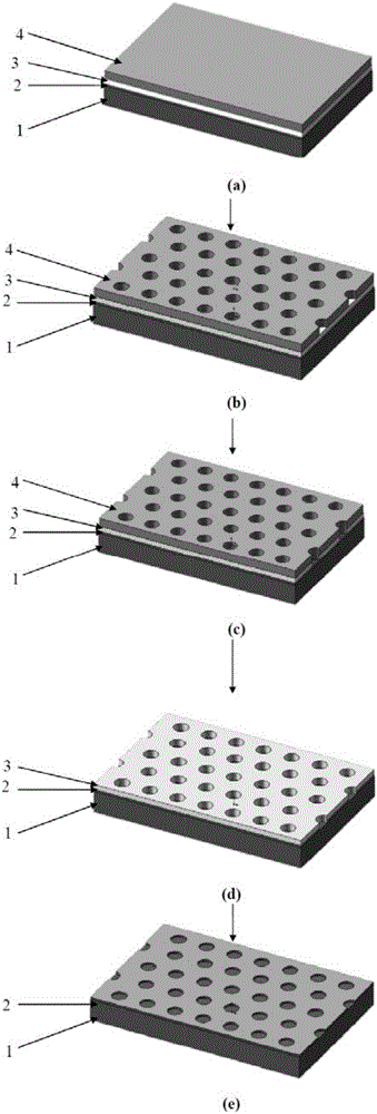
[0036] figure 1 It is a preparation flowchart of a method for preparing a nanoscale graphene structure according to an embodiment of the present invention. see figure 1 , the invention provides a kind of method for preparing the graphene structure of nanoscale, concrete steps comprise:

[0037] Step S1, selecting a substrate 1 and transferring graphene 2 on the substrate 1, or growing graphene 2 on the substrate 1;

[0038] Step S2, vapor-depositing a metal chromium film 3 with a certain thickness on the surface of the graphene 2;

[0039] Step S3, spin-coating an electron beam resist 4 with a certain thickness on the surface of the metal chromium film 3;

[0040] Step S4, using electron beam exposure technology to expose corresponding patterns on the electron beam resist 4, and after developing and fixing, forming nanoscale structural patterns on the electron beam resist 4;

[0041] Step S5, using the electron beam resist 4 with a nanoscale structure pattern as the first ...

Embodiment 1

[0055] Step 1. Select and clean a silicon substrate or a silicon dioxide substrate, and transfer graphene 2 grown by chemical vapor deposition (CVD) on the silicon substrate or silicon dioxide substrate.

[0056] Step 2, using thermal evaporation equipment to grow a metal chromium film 3 with a thickness of 50 nm on the surface of the graphene 2 .

[0057] Step 3: Spin-coat PMMA electron beam resist with a thickness of 200 nm on the surface of the metal chromium film 3 , and bake at 180° C. for 1 minute with a hot plate.

[0058] Step 4, using electron beam exposure equipment to prepare a circular hole array structure with a diameter of 250 nm and a period of 290 nm on the PMMA electron beam resist through exposure, development and fixing.

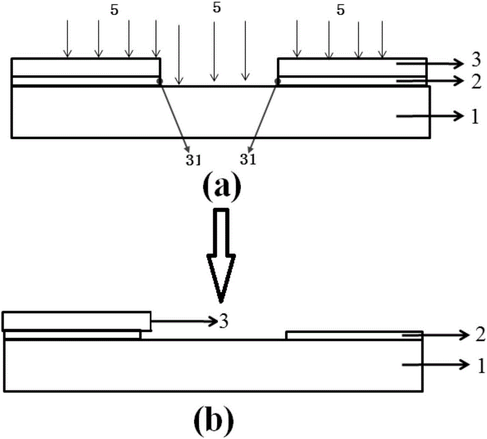
[0059] Step 5. Etching the metal chromium film 3 by using ion beam etching and using the PMMA electron beam resist with a circular hole array structure as the first mask. Among them, the etching beam density is 50mA / cm 3 , the ion energy...

Embodiment 2

[0063] Step 1, select a silicon substrate and wash it, and grow graphene 2 on the silicon substrate by mechanical exfoliation;

[0064] Step 2, using electron beam evaporation equipment to grow a metal chromium film 3 with a thickness of 10 nm on the surface of the graphene 2 .

[0065] Step 3: Spin-coat ZEP520 electron beam resist with a thickness of 50 nm on the surface of the metal chromium film 3, and bake at 180° C. for 2 minutes with a hot plate.

[0066] Step 4. Using electron beam exposure equipment, a circular hole array structure with a diameter of 150 nm and a period of 190 nm can be prepared on the ZEP520 electron beam resist through exposure, development and fixing.

[0067] Step 5, using ion beam etching technology, and using the ZEP520 electron beam resist with a circular hole array structure as the first mask to etch the metal chromium film 3 . Among them, the etching beam density is 100mA / cm 3 , the ion energy is 300eV, and the circular hole array structure ...


PUM

PropertyMeasurementUnit
Thicknessaaaaaaaaaa
Thicknessaaaaaaaaaa
Widthaaaaaaaaaa

Abstract

The invention provides a method for preparing a nano-scale graphene structure and relates to the field of graphene semi-conductor devices. The method comprises specific steps as follows: a metal chromium film is evaporated on the surface of graphene with a substrate; the surface of the metal chromium film is spin-coated with an electron beam resist; an electron beam lithography technique is adopted, a corresponding pattern is exposed on the electron beam resist, and a nano-scale structural pattern is formed on the electron beam resist through developing and fixation; the metal chromium film is etched with the electron beam resist used as a first mask, and a corresponding nano-scale structural pattern is formed on the metal chromium film; the graphene is etched with the metal chromium film used as a second mask, and the size of the graphene can be controlled by controlling etching parameters; the remaining metal chromium film is removed by means of a chromium corrosive liquid, and accordingly, the clean nano-scale graphene structure without impurities is obtained. With the adoption of the method, the feature size of the graphene structure can be controlled under 10 nm, and direct contact of the graphene with the electron beam resist can be avoided.

Description

technical field [0001] The invention relates to the field of graphene semiconductor devices, in particular to a method for preparing a nanoscale graphene structure. Background technique [0002] Due to its excellent properties, such as ultra-high carrier mobility, monoatomic layer thickness, and high mechanical strength, graphene has good potential application value in the field of semiconductors in the future, and has attracted widespread attention. However, since graphene itself has no band gap, in order to realize the application of graphene in the semiconductor field, the problem of opening the band gap must first be solved. The current common method is to cut graphene into nanoribbons. However, the scale of nanobelts generally needs to be below 10nm to realize the application of room temperature semiconductors. [0003] At present, graphene structures with a width of less than 10 nm can be prepared by block copolymer photolithography, but this method is limited by the...

Claims


Application Information

Patent Timeline
IPC IPC(8): C01B31/02C01B31/04H01L21/3065G03F7/20B82Y40/00
CPCB82Y40/00G03F7/20H01L21/3065
Inventor 顾长志张慧珍杨海方唐成春全保刚李俊杰
Owner INST OF PHYSICS - CHINESE ACAD OF SCI
Why Eureka
Try Eureka