Deep ultraviolet light emitting diode chip with high luminous efficiency and preparation method thereof

A light-emitting diode and deep ultraviolet technology, which is applied in semiconductor devices, electrical components, circuits, etc., can solve the problems of AlGaN material doping difficulties, lack of inversion symmetry, and reduced quantum efficiency in light-emitting diode devices, so as to improve the surface Light extraction efficiency, effect of improving ohmic contact performance

Inactive Publication Date: 2016-06-15
HUAZHONG UNIV OF SCI & TECH
View PDF3 Cites 16 Cited by
  • Summary
  • Abstract
  • Description
  • Claims
  • Application Information

AI Technical Summary

Problems solved by technology

[0003] However, the efficiency of deep ultraviolet light-emitting diodes below 315 nanometers is relatively low, and the external quantum efficiency is only less than 15%. AlGaN materials have a high dislocation density (>10 10 cm -2 ), these dislocations may extend to the active region of the quantum well, thereby forming a non-radiative recombination center, and finally the internal quantum efficiency of the LED device is reduced
Second, the doping of AlGaN materials with high Al composition is difficult
Since there is no inversion symmetry, the AlGaN material with wurtzite structure has strong spontaneous polarization and piezoelectric polarization along the [0001] growth direction, and a polarization of MV / cm level can be formed in the quantum well region. The electric field causes the wave functions of electrons and holes to be separated in space, which greatly reduces the radiative recombination rate and reduces the internal quantum efficiency of light-emitting diode devices.
Fourth, it is difficult to emit light from the surface of c-plane AlGaN-based deep ultraviolet light-emitting diodes
[0004] For the above-mentioned problems caused by the crystal field splitting energy band position change and electrode material selection of deep ultraviolet light-emitting diodes, there is still no corresponding system solution in the world to enhance surface light emission. The p-type electrode material generally used is also generally Ti / Al / Ti / Au etc.

Method used


Image

  • Deep ultraviolet light emitting diode chip with high luminous efficiency and preparation method thereof
  • Deep ultraviolet light emitting diode chip with high luminous efficiency and preparation method thereof

Examples


Embodiment 1

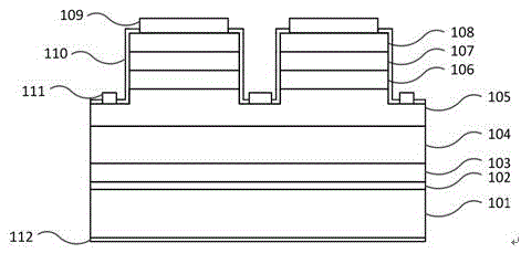
[0017] Such as figure 1 As shown, this embodiment provides a flip-chip deep ultraviolet light-emitting diode chip with high light extraction efficiency, including: a c-plane sapphire substrate 101 thinned to a specific thickness. The Al thin film 112 arranged on the back side of the substrate, the low-temperature AlN nucleation layer 102 arranged on the front side of the substrate, the PALEAlN buffer layer 103 arranged on the low-temperature AlN nucleation layer, and the PALEAlN buffer layer arranged on the The high-temperature AlN intrinsic layer 104 on the high-temperature AlN intrinsic layer, the n-type Al disposed on the high-temperature AlN intrinsic layer x Ga 1-x N layer 105, provided on the n-type Al x Ga 1-x Al on N layer y Ga 1-y N / Al z Ga 1-z The N multi-quantum well layer 106 is arranged on the Al y Ga 1-y N / Al z Ga 1-z p-type Al on N MQW layer u Ga 1-u The N electron blocking layer 107 is arranged on the p-type Al u Ga 1-u The p-type GaN layer 108 o...

Embodiment 2

[0020] This embodiment provides a method for preparing a flip-chip deep ultraviolet light-emitting diode chip with high light extraction efficiency, which specifically includes the following steps:

[0021] (1) On the c-plane sapphire substrate, using the MOCVD process, the substrate temperature is reduced to 600°C, and a low-temperature AlN nucleation layer with a thickness of 20 nm is grown;

[0022] (2) On the low-temperature AlN nucleation layer, increase the growth temperature to 1050° C., and grow a PALEAlN buffer layer with a thickness of 200 nanometers;

[0023] (3) On the PALEAlN buffer layer, increase the growth temperature to 1300° C., and grow a high-temperature AlN intrinsic layer with a thickness of 1000 nanometers;

[0024] (4) On the high-temperature AlN intrinsic layer, keep the growth temperature at 1150 ° C, and grow n-type Al with a thickness of 2500 nm x Ga 1-x N layer, n-type Al x Ga 1-x The N layer is Si doped with a concentration of 10 20 cm -3 Al...


PUM


Abstract

The invention relates to the technical field of semiconductor devices, in particular to a flip-chip deep ultraviolet light-emitting diode chip with high light extraction efficiency and a method for preparing the chip. The flip-chip deep ultraviolet light-emitting diode chip with high light extraction efficiency provided by the present invention selects Ni / Al material with high ultraviolet light reflectivity as the p-type electrode material, which can not only partially improve the ohmic contact performance between the metal electrode and p-type GaN, but also Reflects UV light onto the sapphire facet. The preparation method of the flip-chip deep ultraviolet diode chip with high light extraction efficiency provided by the present invention is to thin the epitaxial sapphire substrate to a specific thickness, and vapor-deposit an Al film with a suitable thickness, through the combination of TM mode ultraviolet light and surface plasmon Coupling partially improves the surface light extraction efficiency of the flip-chip deep ultraviolet light-emitting diode chip.

Description

technical field [0001] The invention relates to the technical field of semiconductor devices, in particular to a flip-chip deep ultraviolet light-emitting diode chip with high light extraction efficiency and a method for preparing the chip. Background technique [0002] AlGaN is a direct bandgap semiconductor material with stable physical and chemical properties. By adjusting the aluminum composition in the material, Al x Ga 1-x The band gap of N(0≤x≤1) varies between 3.4eV(GaN)-6.2eV(AlN), based on Al y Ga 1-y N / Al z Ga 1-z The interband transition of the N quantum well material can realize a 200-365 nanometer adjustable all-solid-state ultraviolet light-emitting diode light source. Compared with traditional mercury lamps, the new AlGaN-based ultraviolet light-emitting diodes have many advantages: 1. The structure of ultraviolet light-emitting diodes is simple, does not contain fragile glass shells, is portable and impact-resistant, and the working voltage is only a fe...

Claims


Application Information

Patent Timeline
Patent Type & Authority Applications(China)
IPC IPC(8): H01L33/40H01L33/20H01L33/00
CPCH01L33/405H01L33/0066H01L33/0075H01L33/20H01L2933/0016
Inventor 王帅陈景文何炬戴江南陈长清
Owner HUAZHONG UNIV OF SCI & TECH
Why Eureka
Try Eureka