Method for preparing oxygen deficiency semiconductor nitrogen dioxide gas-sensitive coating

A nitrogen dioxide and semiconductor technology, used in measuring devices, instruments, material analysis by electromagnetic means, etc., can solve the problems of aging, inconvenient use and application limitations of gas sensors, and achieve absorption, fast response speed, Controlled effect of coating porosity

Inactive Publication Date: 2016-07-06
YANGZHOU UNIV
View PDF11 Cites 10 Cited by
  • Summary
  • Abstract
  • Description
  • Claims
  • Application Information

AI Technical Summary

Problems solved by technology

[0006] Before the present invention was made, most researchers used ultraviolet light as the excitation light source, but it

Method used


Image

  • Method for preparing oxygen deficiency semiconductor nitrogen dioxide gas-sensitive coating
  • Method for preparing oxygen deficiency semiconductor nitrogen dioxide gas-sensitive coating

Examples


Embodiment 1

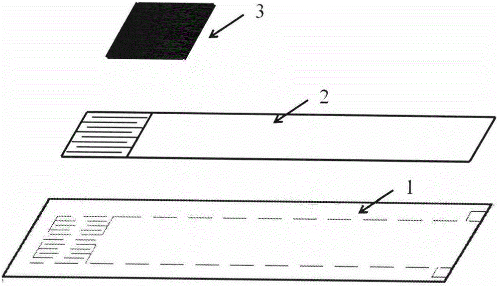
[0051] 1. Use alumina as the insulating substrate 1, wash 30×20×1mm alumina flakes in deionized water and ethanol in turn, and assist with ultrasonic cleaning for 5 minutes, and dry at 80°C for later use.

[0052] 2. Using the method of vacuum coating and metal mask pattern, first prepare a layer of chromium with a thickness of 0.3 μm to improve the bonding strength, and then vapor-deposit a layer of 0.5 μm gold to obtain the interdigitated electrode 2 .

[0053] 3. Weigh 22.14g crystalline zinc acetate Zn (CH 3 COO)·2H 2 O, dissolved in 500ml deionized water, using magnetic stirring to obtain a colorless and transparent solution precursor.

[0054] 4. Using the solution precursor plasma spraying method, spray the ZnO coating directly above the interdigitated electrode, the spraying distance is 75mm, the plasma generation gas is 40ml / min argon and 2ml / min hydrogen, the substrate temperature is room temperature, and the spraying power is 25KW, a ZnO coating with a thickness o...

Embodiment 2

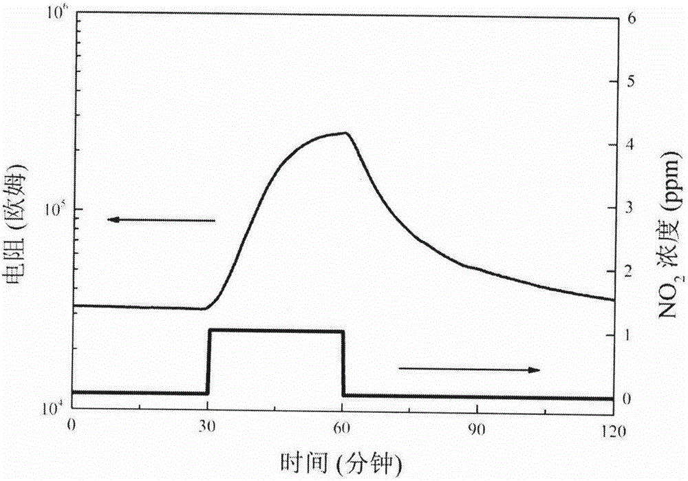
[0060] The difference between this embodiment and embodiment 1 is: in step 3, take by weighing 30.42g crystalline ammonium tungstate, H 40 N 10 o 41 W 12 ·xH 2 O was dissolved in 500ml deionized water, and the colorless and transparent solution precursor was obtained by magnetic stirring; in step 4, the solution plasma spraying method was used to spray WO on the interdigitated electrode 2. 3 Coating, the spraying distance is 100mm, the plasma generation gas is 50mL / min argon and 4mL / min hydrogen, the substrate temperature is 50 degrees, the spraying power is 27KW, and the thickness of 10.0μm is obtained on the interdigitated electrode. 3 coating; the concentration of oxygen defects was 30%, and in step 8, the coating pairs 0.2ppm and 0.5ppmNO 2 When , the sensitivity of the sensor is 3.1 and 5.6 respectively.

Embodiment 3

[0062] The difference between this embodiment and Example 1 is: in step 3, 50.28g crystalline tin dichloride (SnCl 2 ) was dissolved in 500ml deionized water, and a colorless and transparent solution precursor was obtained by magnetic stirring; in step 4, the solution plasma spraying method was used to spray SnO directly above the interdigitated electrode 2 Coating, the spraying distance is 120mm, the plasma generation gas is 40ml / min argon and 3ml / min hydrogen, the substrate temperature is 200 degrees, the spraying power is 26KW, and the SnO with a thickness of 5.0μm is obtained on the interdigitated electrode 2 coating; the concentration of oxygen deficiency was 17%; in step 8, the coating was applied to 2ppm and 5ppmNO 2 , the sensitivities of the sensors were 8.5 and 14.9, respectively.


PUM

PropertyMeasurementUnit
Thicknessaaaaaaaaaa
Thicknessaaaaaaaaaa
Thicknessaaaaaaaaaa

Abstract

The invention relates to a method for preparing an oxygen deficiency semiconductor nitrogen dioxide gas-sensitive coating.A single crystal silicon wafer Si is adopted as an insulating substrate.An interdigitated electrode and a terminal are prepared on the front side of the insulating substrate, inorganic salt powder is dissolved in deionized water or in an organic solvent and stirred to obtain an uniform solution serving as a precursor, the precursor is conveyed to flame flow through a non-atomizing nozzle, the flame flow is generated by a plasma spraying gun, the precursor solution is subjected to evaporation, decomposition, nucleation, heating and acceleration and collided by molten particles, and accordingly the semiconductor gas-sensitive coating is prepared over the interdigitated electrode.The defects in the prior art are overcome.The method can be used for preparing a nano porous structure semiconductor gas-sensitive coating, the coating is ultra-thin, oxygen deficiency concentration in the coating is adjustable, a material band gap is reduced, sensitivity is high, response speed is high, no external heating source is needed, the structure is simple, and reliability is high.

Description

technical field [0001] The invention relates to the technical field of gas sensors in engineering and material science, in particular to a method for preparing an oxygen-deficient semiconductor nitrogen dioxide gas-sensitive coating. Background technique [0002] Nitrogen dioxide (NO 2 ) is an important pollutant that affects air quality. It is a toxic and harmful gas, which mainly comes from urban vehicle exhaust, fuel combustion and industrial production. It can cause a variety of environmental problems in a wide range, and it is one of the main factors in the formation of photochemical smog and one of the sources of acid rain. When the concentration exceeds 200μg / m 3 When exposed, it can cause serious harm to the human respiratory system. my country will implement new ambient air quality standards nationwide on January 1, 2016, and NO 2 Solubility limited to 40μg / m 3 (annual average), so NO 2 Research on gas sensors is quite active. [0003] in NO 2 In gas sensors...

Claims


Application Information

Patent Timeline
IPC IPC(8): G01N27/12
CPCG01N27/127
Inventor 张超耿欣王杰尤佳骏李大玉肖金坤
Owner YANGZHOU UNIV
Why Eureka
Try Eureka