A Method for Immobilizing High Aspect Ratio Micro/Nano Structures Based on Gel Interaction
A technology of micro-nano structure and gelation, applied in micro-structure technology, micro-structure device, manufacturing micro-structure device, etc., can solve problems such as structural failure, achieve the effect of preventing failure, improving yield, and optimizing process parameters
- Summary
- Abstract
- Description
- Claims
- Application Information
AI Technical Summary
Problems solved by technology
Method used
Image
Examples
Embodiment 1
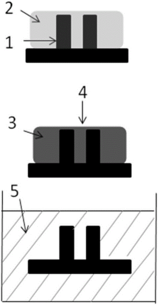
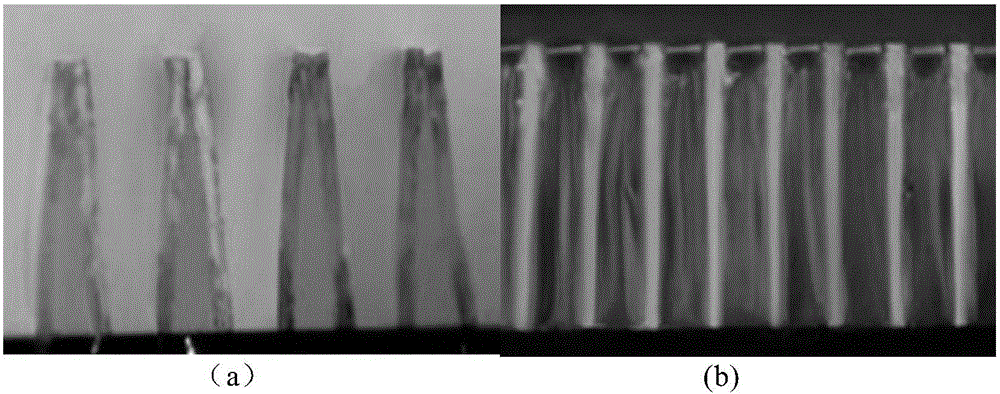
[0028] Example 1, gel immobilization of high aspect ratio micro-nanostructures for observation
[0029] 1. Prepare a hot solution of carrageenan with a mass concentration of 1%: 1g of carrageenan, 100ml of water, and heat to dissolve at 90°C;
[0030] 2. Take the 2-inch silicon wafer containing the micro-nano structure with large aspect ratio out of the developer solution and place it in deionized water. Take it out after 1 minute, and quickly add 5 ml of prepared gellan gum on the surface to heat it. solution;
[0031] 3. At room temperature, first put the silicon wafer on the gel-spinning table to cool for 30 seconds, and then spin-coat according to the set gel-spinning machine parameters: first spin-coat at 1000r / min for 10 seconds; then spin at 2000r / min Apply for 20 seconds. After the spin coating is completed, let it stand for 1 minute to obtain a fixed gel layer and form a gel-fixed micro-nano structure;
[0032] 4. Observe the silicon wafer under a microscope, and c...
Embodiment 2
[0034] Example 2, gel immobilization of large aspect ratio micro-nanostructures for electroplating
[0035] 1. Prepare gellan gum hot solution with a concentration of 0.6%: gellan gum 0.6g, water 100ml, heat to dissolve at 80°C;
[0036] 2. Take the 2-inch silicon wafer containing the micro-nano structure with large aspect ratio out of the developer solution and place it in deionized water. Take it out after 1 minute, and quickly add 5 ml of prepared gellan gum on the surface to heat it. solution;
[0037] 3. At room temperature, first put the silicon wafer on the gel-spinning table to cool for 30 seconds, and then spin-coat according to the set gel-spinning machine parameters: first spin-coat at 1000r / min for 10 seconds; then spin at 2000r / min Apply for 20 seconds. After the spin coating is completed, let it stand for 30 seconds to obtain a fixed gel layer and form a gel-fixed micro-nano structure;
[0038] 4. After placing the silicon wafer under a microscope for observat...
Embodiment 3
[0041] Example 3, gel immobilization of large aspect ratio micro-nanostructures for observation
[0042] 1. Prepare a carrageenan hot solution with a mass concentration of 0.8%: carrageenan 0.8g, water 100ml, heat to dissolve at 90°C;
[0043] 2. Take out the 2-inch silicon wafer containing the micro-nano structure with large aspect ratio from the developer solution and place it in deionized water, take it out after 1 minute, and quickly put it into the prepared hot carrageenan solution;
[0044] 3. After standing for 1 minute, pull up the silicon wafer vertically at a speed of 5mm / s, and let it stand for 5 minutes at room temperature to obtain a fixed gel layer and form a gel-fixed micro-nano structure;
[0045] 4. Observe the silicon wafer under a microscope, and conduct process evaluation by detecting the micro-nano structure;
[0046] 5. Place the observed silicon wafer in an 80°C water bath and shake gently for 2 minutes, and the gel between the micro-nano structures can b...
PUM
 Abstract
Description
Claims
Application Information

