Heat sink material and preparation method thereof

A heat sink material and combined technology, applied in chemical instruments and methods, layered products, metal layered products, etc., can solve the problem of heat sink materials that cannot be applied to micro-nano optoelectronic devices, mold-based direct molding preparation is difficult to achieve, Unable to directly apply heat sink materials and other issues to achieve high thermal conductivity, low cost, and easy operation

Inactive Publication Date: 2016-10-05
LANZHOU INST OF PHYSICS CHINESE ACADEMY OF SPACE TECH
View PDF5 Cites 11 Cited by
  • Summary
  • Abstract
  • Description
  • Claims
  • Application Information

AI Technical Summary

Problems solved by technology

However, diamond is expensive and difficult to process, and it is difficult for a single diamond to be directly used as a heat sink material
Generally, diamond particles are combined with copper, aluminum and other metal materials to prepare composite heat sink materials, and the thermal conductivity is about 400-800 W/mK. However, there are great difficulties in the miniaturization process of this composite heat sink material. It is very difficult to process, and it is also difficult to realize the direct molding preparation of the mold,

Method used


Image

  • Heat sink material and preparation method thereof
  • Heat sink material and preparation method thereof
  • Heat sink material and preparation method thereof

Examples


Embodiment 1

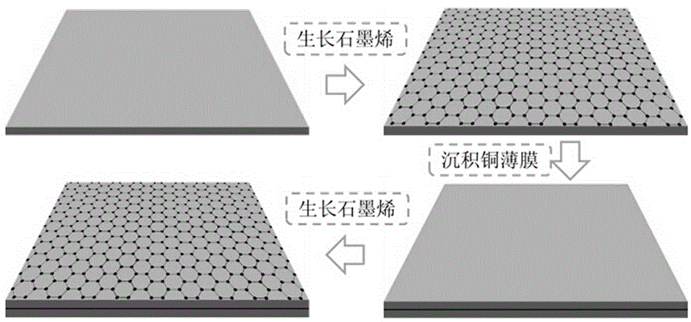
[0029] The preparation process of the present invention is as figure 1 shown, including the following steps:

[0030] a. Using aluminum foil as the substrate, first prepare a copper thin film layer on the aluminum foil by vacuum evaporation method and a vacuum coating machine, and control the vacuum degree of the background to 10 -2 Pa, the temperature is 1500°C, and a copper thin film layer with a thickness of 500nm is deposited on the aluminum foil;

[0031] b. Using the chemical vapor deposition method and using a horizontal reactor to grow graphene on the copper film layer, using methane and hydrogen as the growth precursors, the methane flow rate is 20 sccm, the hydrogen gas flow rate is 50 sccm, the growth temperature is 1000 ° C, and the growth time is 30 minutes. Graphene is directly grown on the copper film to form a graphene layer;

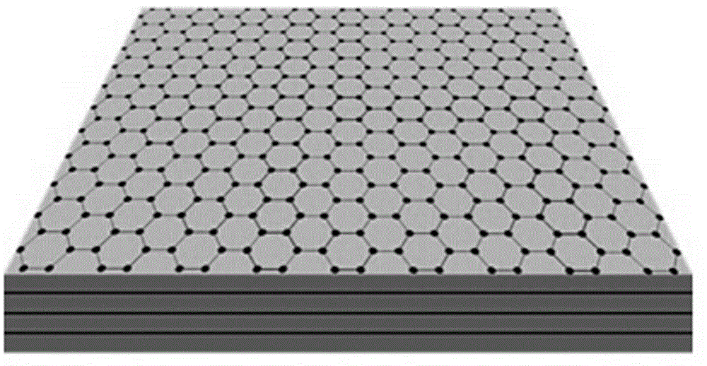
[0032] c. After the growth is completed, the vacuum evaporation method is used to prepare a copper thin film layer through a vacuum ...

Embodiment 2

[0038] The preparation process of the present invention is as figure 1 shown, including the following steps:

[0039] a. Using aluminum foil as the substrate, first prepare a copper thin film layer on the aluminum foil by vacuum evaporation method and a vacuum coating machine, and control the vacuum degree of the background to 10 -2 Pa, the temperature is 1500°C, and a copper film layer with a thickness of 200nm is deposited on the aluminum foil;

[0040] b. Using the chemical vapor deposition method and using a horizontal reactor to grow graphene on the copper film layer, using methane and hydrogen as the growth precursors, the methane flow rate is 20 sccm, the hydrogen gas flow rate is 50 sccm, the growth temperature is 1000 ° C, and the growth time is 30 minutes. Graphene is directly grown on the copper film to form a graphene layer;

[0041] c. After the growth is completed, the vacuum evaporation method is used to prepare a copper thin film layer through a vacuum coati...

Embodiment 3

[0047] The preparation process of the present invention is as figure 1 shown, including the following steps:

[0048] a. Using nickel foil as the substrate, first adopt the vacuum evaporation method on the nickel foil and prepare the copper thin film layer through a vacuum coating machine, and control the vacuum degree of the background to be 10-2 Pa, the temperature is 1500°C, and a copper film layer with a thickness of 200nm is deposited on the nickel foil;

[0049] b. Graphene is transferred on the copper film layer by graphene transfer method to form a graphene layer. The transfer process of the graphene transfer method is as follows: 1) First cut the copper foil with graphene into a square piece of 10×10cm; 2) Spin a layer of plexiglass with a spin coater at a speed of 3000 rpm for 1 min ;3) Drying treatment, temperature 100℃, time 30min; 4) Copper foil with graphene spin-coated with plexiglass on the upper surface was put into 20% nitric acid solution to corrode copper...


PUM

PropertyMeasurementUnit
Thicknessaaaaaaaaaa

Abstract

The invention relates to a heat sink material, in particular to a heat sink material applied to micro-nano-scale power devices such as micro-nano optoelectronic devices and a preparation method of the heat sink material. The heat sink material comprises three or more copper film layers and three or more graphene layers, wherein the copper film layers and the graphene layers are combined together in an alternative mode. According to the heat sink material and the preparation method thereof, the multilayer stacking structure of copper/graphene is adopted, and the composite heat sink material with the multi-stacking layers of copper/graphene is obtained by preparing the copper films and graphene alternatively. The superhigh heat conductivity characteristic of graphene is utilized, graphene is directly grown on the copper film layers, the problem that graphene of a planar structure cannot be directly applied to heat sink materials is solved, and high heat conductivity can be achieved; meanwhile, the heat sink material has very high processibility through combination of graphene and copper.

Description

technical field [0001] The invention relates to a heat sink material, in particular to a heat sink material applied to micro-nano-scale power devices such as micro-nano optoelectronic devices, and a preparation method thereof. Background technique [0002] In the past few decades, the continuous pursuit of the function and performance of microelectronic devices has made them develop in the direction of high density, high power and high speed, and their volume is also developing in the direction of miniaturization. At present, the feature size of semiconductors has tended to 100nm, which means that millions of micro devices can be used to complete the structure of chips. According to this trend, the heat generation will continue to increase, and the heat flux of a single chip will far exceed 100W / cm 2 , multi-chip modules will exceed 25 W / cm 2 , while the printed circuit board will exceed 10 W / cm 2 , this high-density and high-power demand makes microelectronic heat dissip...

Claims


Application Information

Patent Timeline
IPC IPC(8): B32B15/04B32B9/04
Inventor 郭磊陈学康王兰喜曹生珠车清论
Owner LANZHOU INST OF PHYSICS CHINESE ACADEMY OF SPACE TECH
Why Eureka
Try Eureka