Two-dimensional black phosphorus/transitional metal chalcogenide heterojunction device and preparation method therefor

A transition metal chalcogenide and compound technology, applied in the field of microelectronics, can solve problems such as being unsuitable for heterojunction, and achieve the effects of simple preparation method, simple and easy method, and small contact resistance

Inactive Publication Date: 2016-10-12
TIANJIN UNIVERSITY OF TECHNOLOGY
View PDF3 Cites 77 Cited by
  • Summary
  • Abstract
  • Description
  • Claims
  • Application Information

AI Technical Summary

Problems solved by technology

[0003] Among the two-dimensional materials, graphene, as the focus of most attention at present, is not sui

Method used


Image

  • Two-dimensional black phosphorus/transitional metal chalcogenide heterojunction device and preparation method therefor
  • Two-dimensional black phosphorus/transitional metal chalcogenide heterojunction device and preparation method therefor
  • Two-dimensional black phosphorus/transitional metal chalcogenide heterojunction device and preparation method therefor

Examples


Embodiment 1

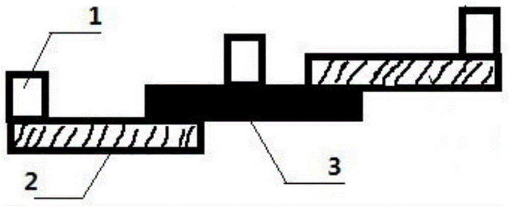
[0028] A device based on a two-dimensional black phosphorus / transition metal chalcogenide heterojunction, such as figure 1 As shown, the heterojunction is two-dimensional black phosphorus nanoflakes and two-dimensional transition metal chalcogenide MoS 2 Nano-flake stack structure, the number of layers of two-dimensional black phosphorus is 5 layers, two-dimensional MoS 2 The thickness of the nanosheet is 8 layers, the material of the device electrode is 80nm Au, and the substrate of the device is a silicon oxide sheet, SiO 2 The thickness is 270nm.

[0029] Based on the two-dimensional black phosphorus / MoS 2 Heterojunction devices are used to prepare bipolar transistors, the steps are as follows:

[0030] 1) Mechanically exfoliate the black phosphorus single crystal to obtain a two-dimensional black phosphorus nanosheet with 5 layers, which is used as the base of the transistor;

[0031] 2) Preparation of two-dimensional MoS by atmospheric pressure chemical vapor depositi...

Embodiment 2

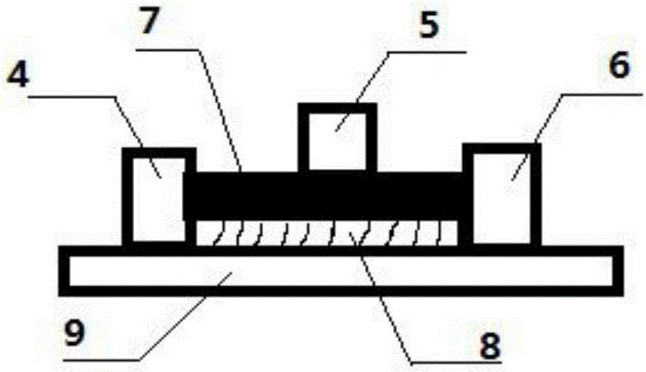
[0037] A device based on a two-dimensional black phosphorus / transition metal chalcogenide heterojunction, such as figure 2 As shown, the heterojunction is two-dimensional black phosphorus nanoflakes and two-dimensional MoS 1.6 Se 0.4 Nano-flake stack structure, the number of layers of two-dimensional black phosphorus is 2 layers, two-dimensional MoS 1.6 Se 0.4 The thickness of the nanoflakes is 1 layer, that is, for MoS 2 Doping with Se, the material of the device electrode is 80nm metal Au, the substrate of the device is a silicon oxide wafer, SiO 2 The thickness is 270nm.

[0038] The two-dimensional black phosphorus / transition metal chalcogenide based heterojunction device is used to prepare a field effect transistor, and the steps are as follows:

[0039] 1) Mechanical exfoliation of black phosphorus single crystals to obtain bilayer two-dimensional black phosphorus nanoflakes in heterojunctions;

[0040] 2) Preparation of two-dimensional monolayer MoS by atmospheri...

Embodiment 3

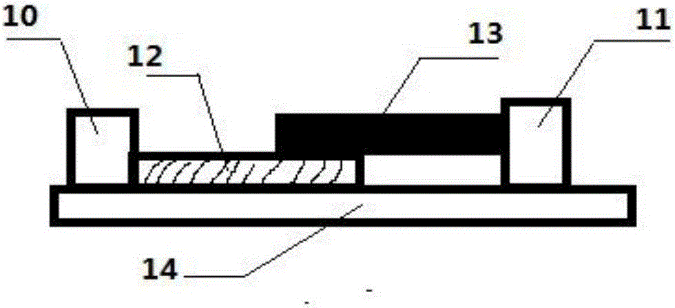
[0046] A device based on a two-dimensional black phosphorus / transition metal chalcogenide heterojunction, such as image 3 As shown, the heterojunction is two-dimensional black phosphorus nanosheets and two-dimensional WS 2 Nano-flake stack structure, the number of layers of two-dimensional black phosphorus is one layer, two-dimensional WS 2 The thickness of the nanosheet is 1 layer, the electrode material of the device is 80nm conductive metal Au, and the substrate of the device is a silicon oxide sheet, SiO 2 The thickness is 270nm.

[0047] The two-dimensional black phosphorus / transition metal chalcogenide based heterojunction device is used to prepare a photodetector / photodiode, and the steps are as follows:

[0048] 1) Mechanical exfoliation of black phosphorus single crystals to obtain two-dimensional black phosphorus nanoflakes in heterojunctions;

[0049] 2) Preparation of 2D WS by atmospheric pressure chemical vapor deposition 2 Nano flakes, its preparation proces...


PUM

PropertyMeasurementUnit
Thicknessaaaaaaaaaa
Thicknessaaaaaaaaaa

Abstract

The invention discloses a two-dimensional black phosphorus/transitional metal chalcogenide heterojunction based device. The heterojunction adopts a laminated structure of two-dimensional black phosphorus nanometer slices and two-dimensional transitional metal chalcogenide nanometer slices; the number of the two-dimensional black phosphorus layers is 1-50; the two-dimensional transitional metal chalcogenide comprises 1-50 layers in terms of thickness; the two kinds of two-dimensional materials are prepared and synthesized through chemical vapor deposition, mechanical stripping, liquid phase stripping and the like; and the device can be used for preparing a bipolar transistor, a field effect transistor or a photoelectric detector/photoelectric diode. The two-dimensional black phosphorus/transitional metal chalcogenide heterojunction device has the advantages as follows: a combination of the two kinds of two-dimensional materials of black phosphorus and the transitional metal chalcogenide is adopted to form the brand new pn type heterojunction structure; the heterojunction is combined based on natural van der Waals forces among materials; compared with the conventional heterojunction epitaxial growth process, the heterojunction device provided by the invention is easier to prepare; and compared with the existing bulk material, the heterojunction device provided by the invention is smaller in size, thinner, higher in flexibility and higher in the integration degree, so that the two-dimensional black phosphorus/transitional metal chalcogenide heterojunction device has the potential to be applied to the wearable equipment in the future.

Description

technical field [0001] The invention belongs to the technical field of microelectronics, and specifically relates to a two-dimensional black phosphorus / transition metal chalcogenide heterojunction device and a preparation method thereof. Background technique [0002] As the development of silicon-based material integrated circuits is limited by physical size, two-dimensional nanomaterials such as graphene, transition metal sulfides, and black phosphorus have attracted more and more attention from scientists. They can be used to manufacture materials that surpass silicon-based materials. Optoelectronic devices with limited physical size, smaller volume and better performance. For example: Yang Naiyun's patent of Shanghai Electric Power Institute, a flexible two-dimensional material light-emitting device (CN 105185884 A), focuses on MoS 2 The flexible characteristics; another example is that in 2011, B.Radisavljevic, A.Radenovic and others used single-layer MoS 2 A field eff...

Claims


Application Information

Patent Timeline
IPC IPC(8): H01L29/06H01L29/24H01L29/735H01L29/737H01L21/34H01L29/78H01L31/032H01L31/0352H01L31/072H01L31/18B82Y30/00B82Y40/00
CPCB82Y30/00B82Y40/00H01L29/0665H01L29/24H01L29/66969H01L29/735H01L29/737H01L29/78H01L31/032H01L31/035281H01L31/072H01L31/18Y02E10/50Y02P70/50
Inventor 张楷亮唐登轩冯玉林王芳方明旭李悦韩叶梅邢宇鹏
Owner TIANJIN UNIVERSITY OF TECHNOLOGY
Why Eureka
Try Eureka