Memory storage device based on carbon dot/organic polymer composite material

A composite material, memory storage technology, applied in the field of new organic storage materials, can solve problems such as no reports, and achieve excellent performance, long retention time, and good stability.

Inactive Publication Date: 2016-10-19
TECHNICAL INST OF PHYSICS & CHEMISTRY - CHINESE ACAD OF SCI
View PDF9 Cites 4 Cited by
  • Summary
  • Abstract
  • Description
  • Claims
  • Application Information

AI Technical Summary

Problems solved by technology

Due to its biocompatibility and unique characteristics, carbon quantum dots also have many applications in the field of biomarkers, but the application of carbon quantum dots to memory storage devices has not been reported yet.

Method used


Image

  • Memory storage device based on carbon dot/organic polymer composite material
  • Memory storage device based on carbon dot/organic polymer composite material
  • Memory storage device based on carbon dot/organic polymer composite material

Examples


Embodiment 1

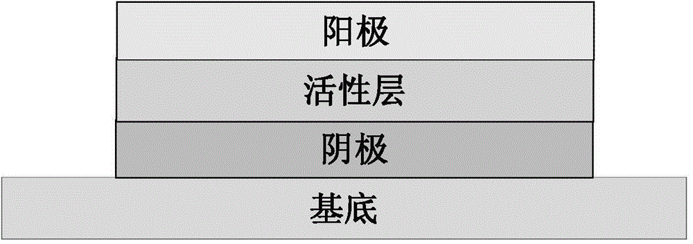
[0049] A method for preparing a two-terminal diode memory storage device, comprising the following steps:

[0050] 1) Dissolving a blend of polyvinyl alcohol PVA and carbon dots doped with N heteroatoms in an aqueous solution at a weight ratio of 50:1 to obtain a mixed solution, which is a composite material;

[0051] 2) Deposit cathode electrode material gold on the surface of indium tin oxide transparent conductive glass, spin-coat the composite material obtained in 1) onto the surface of the gold electrode to form an active layer, and the thickness of the active layer is about 70nm;

[0052] After that, anneal at 100°C for 30min;

[0053] Finally, a metal silver electrode (thickness 100nm) is deposited on the surface of the active layer under vacuum by a coating machine to obtain a nonvolatile two-terminal diode memory device based on heteroatom-doped carbon dots.

[0054] Measured switch ratio up to 10 5 .

[0055] The structural formula of polyvinyl alcohol PVA is as f...

Embodiment 2

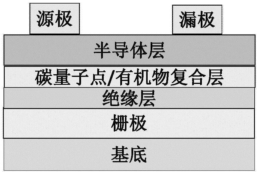
[0061] A preparation method for a three-terminal memory storage device, comprising the following steps:

[0062] (1) Deposit gate (gold) and insulating layer (silicon dioxide) sequentially on the base material ITO substrate according to conventional methods;

[0063] (2) Dissolving polyvinyl alcohol PVA and carbon dots doped with S heteroatoms in methanol at a weight ratio of 2:1 to obtain a mixed solution, which is a composite material;

[0064] (3) The composite material is deposited on the surface of the insulating layer by spin coating, printing, etc. to form a charge trapping layer;

[0065] Using a semiconductor film forming method, depositing pentacene material on the surface of the charge trapping layer to form a semiconductor layer with a thickness of 10nm;

[0066] Depositing at least one layer of patterned silver, copper, gold and other metals on the surface of the semiconductor layer to form source and drain electrodes;

[0067] Obtained a non-volatile three-term...

Embodiment 3

[0071] A method for preparing a two-terminal diode memory storage device, comprising the following steps:

[0072] 1) Organic polymer (poly-p-phenylene vinylene, a mixture of poly-p-phenylene vinylene derivatives, polyacetylene and polyacetylene derivatives in a weight ratio of 1:2:2:1) and carbon The point blend was stirred in an aqueous solution at a weight ratio of 50:1 at 30°C for 10 minutes to obtain a mixed solution, which was a composite material; the concentration of the organic polymer was 10 mg / ml;

[0073] 2) Deposit the silver cathode electrode material on the surface of the silicon base material, pull the composite material obtained in step 1) to the surface of the silver cathode electrode material to form an active layer (thickness is 20nm), then anneal at 60°C for 10min, and finally use a coating machine on the surface of the silver cathode electrode material. The anode electrode material ITO (thickness: 20nm) was evaporated on the surface of the active layer un...


PUM

PropertyMeasurementUnit
concentrationaaaaaaaaaa
thicknessaaaaaaaaaa
thicknessaaaaaaaaaa

Abstract

The invention discloses a memory storage device based on a carbon dot / organic polymer composite material. The memory storage device comprises a layer made from a carbon dot / organic polymer composite material, wherein the composite material is a compound of a carbon dot and organic polymer; the carbon dot is the heteroatom-doped carbon dot or the non-heteroatom-doped carbon dot; and the organic polymer is one selected from or is a compound formed by more than two polymers selected from polyvinyl alcohol, a polyvinyl alcohol derivative, poly(p-phenylene vinylene), a poly(p-phenylene vinylene) derivative, polyacetylene, a polythiophene derivative, polythiophene, a polythiophene derivative, fullerenes and a fullerene derivative. According to the invention, the memory storage device has excellent performances; the switch ratio reaches 105; the retention time is long; and the stability is high.

Description

technical field [0001] The invention relates to the field of new organic storage materials. More specifically, it relates to a memory storage device based on carbon dots / organic polymer composites. Background technique [0002] With the development of information technology, the storage of a large amount of digital information has higher and higher requirements for storage devices. The high performance, low cost and easy processing of devices have always been the constant pursuit of goals in this field. In recent decades, although the earliest non-volatile memory storage devices based on inorganic semiconductors such as silicon and germanium have high performance, their expensive preparation costs and complex process conditions have increasingly limited their further development. Especially under the current trend of rapid development of flexible and wearable devices, the disadvantages of memory storage devices based on inorganic materials are becoming increasingly prominen...

Claims


Application Information

Patent Timeline
Patent Type & Authority Applications(China)
IPC IPC(8): H01L51/00H01L27/10G11C13/00
Inventor 王鹰汪鹏飞孟令强刘卫敏葛介超
Owner TECHNICAL INST OF PHYSICS & CHEMISTRY - CHINESE ACAD OF SCI
Why Eureka
Try Eureka