Method for preparing black silicon by wet process

A black silicon, wet process technology, applied in the field of solar cells, to solve the bottleneck of mass industrialization, improve absorption efficiency, and achieve the effect of good compatibility

Active Publication Date: 2016-11-09
SUNFONERGY ALTERNATIVE ENERGY TECH
View PDF11 Cites 15 Cited by
  • Summary
  • Abstract
  • Description
  • Claims
  • Application Information

AI Technical Summary

Problems solved by technology

[0010] However, the suede obtained by the above methods has a mixed structure of micron

Method used


Image

  • Method for preparing black silicon by wet process
  • Method for preparing black silicon by wet process
  • Method for preparing black silicon by wet process

Examples


Embodiment 1

[0037] Wet black silicon preparation, the steps are as follows:

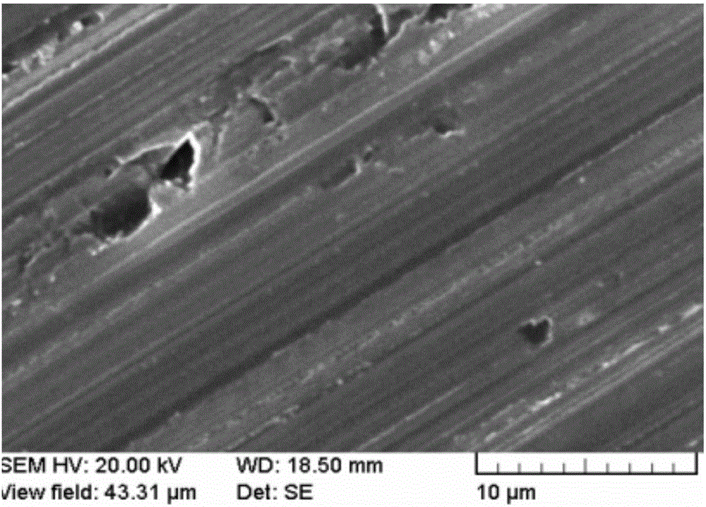
[0038] (1) Select a P-type polysilicon wafer (boron-doped, 1-3Qcm, 156X156mm square, thickness 180μm), because the polysilicon wafer is cut with a diamond wire saw, so the damage during slicing remains on the surface. Add 2% mass additives of NaOH aqueous solution to 3% NaOH aqueous solution, immerse the silicon chip in the above aqueous solution, and corrode in the solution at 65°C for 300 seconds to make the silicon surface structure of the damaged layer uniform and reduce anisotropic scars.

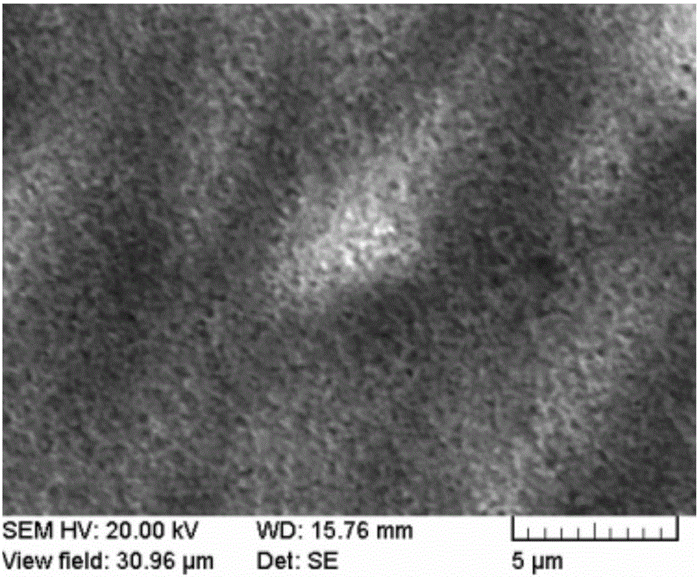
[0039] (2) Rinse the product wafer of step (1) with deionized water; after drying, put it into the metal ion aqueous solution and attach it for 300 seconds at room temperature; wherein, the metal ion is derived from HAuCl 4 and AgNO 3 The combination of HAuCl4 and AgNO3 are electronic grade products. The weight ratio of HAuCl4 to AgNO3 is 1:6, and the total content of HAuCl4 and AgNO3 in the solution is 0.01mol / L. In ...

Embodiment 2

[0047] Wet black silicon preparation, the steps are as follows:

[0048] (1) Select a P-type polysilicon wafer (boron-doped, 1-3Qcm, 156X156mm square, thickness 180μm), because the polysilicon wafer is cut with a diamond wire saw, so the damage during slicing remains on the surface. Add 2% mass additives of NaOH aqueous solution to 3% NaOH aqueous solution, immerse the silicon chip in the above aqueous solution, and corrode in the solution at 65°C for 300 seconds to make the silicon surface structure of the damaged layer uniform and reduce anisotropic scars.

[0049] (2) Rinse the product wafer of step (1) with deionized water; after drying, put it into the metal ion aqueous solution and attach it for 240 seconds at room temperature; wherein, the metal ion is derived from HAuCl 4 and AgNO 3 The combination of HAuCl4 and AgNO3 are electronic grade products. The weight ratio of HAuCl4 to AgNO3 is 5:1.2, and the total content of HAuCl4 and AgNO3 in the solution is 0.005mol / L. ...

Embodiment 3

[0057] Wet process black silicon preparation method, comprises the following steps:

[0058] (1) Immerse the silicon wafer in a 3% sodium hydroxide or potassium hydroxide solution containing additives, the additive amount is 3% of the mass of the alkali solution, and polish the silicon wafer at 50°C for 180 seconds to remove the surface damage of the silicon wafer layer; add additives to avoid sticking bubbles during the corrosion process and cause unclean surfaces;

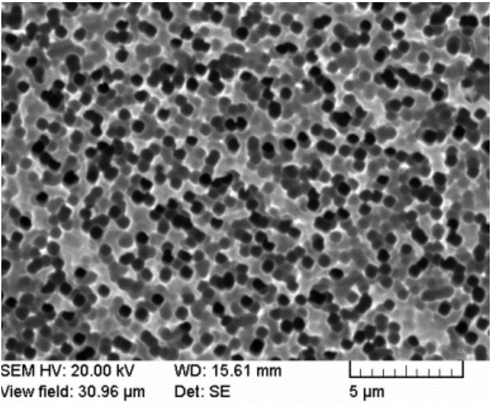
[0059] (2) Immerse the polished silicon chip in a metal ion solution with a concentration of 0.025mol / L for 100 seconds at normal temperature, so that the metal ion is attached to the silicon chip; the metal ion is a combination of platinum ion and palladium ion; during the attachment process, also Add concentrated hydrofluoric acid and a high molecular weight polymer with a molecular weight of 10000, the concentration of the high molecular polymer is 25ppm, and the mass percentage concentration of the concentrat...


PUM

PropertyMeasurementUnit
Concentrationaaaaaaaaaa

Abstract

The invention provides a method for preparing black silicon by a wet process. The method comprises the following steps of: soaking a silicon wafer into an additive-contained alkaline solution, and polishing the silicon wafer to remove a damaged layer on a surface of the silicon wafer; soaking the polished silicon wafer into a metal ion solution so that metal ions are adhered to the silicon wafer; soaking the silicon wafer adhered with the metal ions into a mixed solution of concentrated hydrofluoric acid and an oxidant for reaction to obtain black silicon; and soaking the black silicon into a mixed acid solution containing an additive or a slow-release agent to obtain the silicon wafer with a uniform texture surface of a sub-micrometer structure. The method is simple in process, the prepared silicon wafer has a relatively low reflectivity of 7%-15%, the absorption efficiency of a silicon cell for light is greatly improved, and thus the conversion efficiency of a solar cell is enhanced.

Description

technical field [0001] The invention belongs to the field of solar cells, in particular to a preparation method of wet black silicon. Background technique [0002] The reflection of incident light on the surface of the silicon wafer greatly reduces the efficiency (current flow) of silicon solar cells. If there is no anti-reflection treatment on the surface of the silicon cell, about 40% of the sunlight will be lost. This antireflection effect must be effective across the entire solar spectrum and at a wide variety of incident light angles. [0003] Currently, antireflection on crystalline silicon photovoltaic cells is achieved through several different techniques. For monocrystalline silicon, anisotropic (pyramidal) texture etched silicon single crystals reduce reflectivity to about 5-15% above facing 100 monocrystalline silicon, but mainly at incident light angles close to 90° rather than reflection at low incidence angles Rate. This technique also consumes a large amou...

Claims


Application Information

Patent Timeline
IPC IPC(8): H01L31/18
CPCH01L31/02363Y02E10/50Y02P70/50
Inventor 韩冰丁晓辉韩庚欣徐涛
Owner SUNFONERGY ALTERNATIVE ENERGY TECH
Why Eureka
Try Eureka