Semiconductor device manufacturing method, semiconductor device and electronic device

A manufacturing method, semiconductor technology, applied in the direction of semiconductor devices, semiconductor/solid device manufacturing, semiconductor/solid device components, etc., can solve the impact of electrical conductivity, affect aluminum pads and the first metal layer, large expansion, etc. problems, to avoid oxidation, reduce thermal mismatch, and reduce internal stress

Active Publication Date: 2019-02-01
SEMICON MFG INT (SHANGHAI) CORP
View PDF4 Cites 0 Cited by
  • Summary
  • Abstract
  • Description
  • Claims
  • Application Information

AI Technical Summary

Problems solved by technology

figure 2 It shows the problem of copper bumps in the TSV via hole, the main reason is that the copper volume expands during the heating process, the volume of copper in the TSV hole is very large, resulting in a large amount of expansion, and the protruding part affects the aluminum above it Pad and first metal layer
[0004] In production, such problems are usually alleviated by adjusting the ingredients (recipe) in the process, and the yield and reliability are improved. However, the fundamental reasons such as copper / silicon differences and excessive copper volume still exist. Therefore, these problems can still happen
In addition, there are currently methods to alleviate this problem by thickening the SiO2 layer or adding some plastic materials, such as benzocyclobutene (BCB), etc. to absorb the internal stress of copper, but in the smaller TSV structure, adding these non- Conductive materials may have some influence on their ability to conduct electricity

Method used


Image

  • Semiconductor device manufacturing method, semiconductor device and electronic device
  • Semiconductor device manufacturing method, semiconductor device and electronic device
  • Semiconductor device manufacturing method, semiconductor device and electronic device

Examples


Embodiment 1

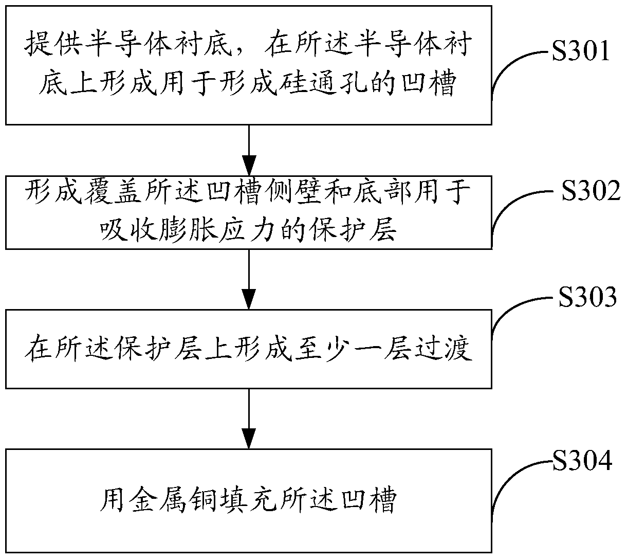
[0045] Combine below Figure 4A ~ Figure 4F The manufacturing method of the semiconductor device of the present invention is described in detail.

[0046] First, if Figure 4A As shown, a semiconductor substrate 400 is provided, and a groove 401 for forming a through silicon via is formed on the semiconductor substrate 400 . The semiconductor substrate 400 may be at least one of the materials mentioned below: silicon, germanium. In addition, other devices, such as PMOS and NMOS transistors, may be formed on the semiconductor substrate. An isolation structure may be formed in the semiconductor substrate, and the isolation structure is a shallow trench isolation (STI) structure or a local oxide of silicon (LOCOS) isolation structure. CMOS devices may also be formed in the semiconductor substrate, such as transistors (eg, NMOS and / or PMOS) and the like. Similarly, a conductive member may also be formed in the semiconductor substrate, and the conductive member may be the gate,...

Embodiment 2

[0066] The present invention also provides a semiconductor device fabricated by the method described in Embodiment 1, a semiconductor substrate 500, a groove 501 formed on the semiconductor substrate 500 for forming through-silicon vias, and a groove 501 formed in the groove A protective layer 502 for absorbing expansion stress, at least one transition layer and a metal copper layer 506 are sequentially formed in 501, wherein the transition layer is made of a metal material, and the thermal expansion coefficient of the transition layer is smaller than that of copper.

[0067] Preferably, the transition layer is multi-layered, and the thermal expansion coefficient of each transition layer increases gradually along the direction away from the protective layer.

[0068] As an example, in this embodiment, the transition layer includes a first transition layer 503 , a second transition layer 504 and a third transition layer 505 sequentially formed on the protective layer 502 , and t...

Embodiment 3

[0073] The present invention further provides an electronic device including the aforementioned semiconductor device.

[0074] The electronic device can be any electronic product or equipment such as mobile phone, tablet computer, notebook computer, netbook, game console, TV, VCD, DVD, navigator, camera, video recorder, voice recorder, MP3, MP4, PSP, etc. It is an intermediate product with the above-mentioned semiconductor device, for example: a mobile phone motherboard with the integrated circuit, etc. In this implementation, take PDA as an example, such as Image 6 shown.


PUM


Abstract

The invention provides a manufacturing method for a semiconductor device. The manufacturing method comprises: a semiconductor substrate is provided and a groove for forming a through silicon via is formed in the semiconductor substrate; a protection layer that covers the side wall and the bottom of the groove and is used for absorbing a swelling stress is formed; at least one transition layer is formed on the protection layer; and the groove is filled by metallic copper, wherein the transition layer employs a metal material and the thermal expansion coefficient of the transition layer is smaller than that of the copper. According to the manufacturing method, the metal material having the small thermal expansion coefficient is added between the silicon and cooper during the through silicon via forming process to form the transition layer between the Si / Cu, so that the thermal mismatching between the two kinds of materials is reduced; the thermal expansion coefficient is increased gradually from the transition layer to the metallic copper layer, thereby reducing the thermal mismatching among all materials at all layers effectively and thus avoiding layering or copper layer protrusion.

Description

technical field [0001] The present invention relates to the technical field of semiconductors, in particular to a manufacturing method of a semiconductor device, a semiconductor device and an electronic device. Background technique [0002] In the field of semiconductor technology, through-silicon via (TSV) technology is the key to realizing vertical interconnection. The 3D integration method using TSV technology can improve the integration level of devices, data exchange speed and signal speed, reduce interconnection length, reduce power consumption and improve In terms of performance such as input / output density, it is also possible to realize multi-functional integrated packaging such as memory, dedicated IC, and processing area in one package. [0003] In wafers with through-silicon vias (TSVs), metal copper is usually used to fill the TSVs for interconnection. However, due to the large difference between the physical properties of copper and silicon, the use of large v...

Claims


Application Information

Patent Timeline
Patent Type & Authority Patents(China)
IPC IPC(8): H01L21/768H01L23/48
Inventor 李广宁沈哲敏
Owner SEMICON MFG INT (SHANGHAI) CORP
Why Eureka
Try Eureka