Heterojunction solar cell taking silicon nanorod array as substrate and fabrication method of heterojunction solar cell

A technology of silicon nanopillars and solar cells, applied in circuits, photovoltaic power generation, electrical components, etc., can solve problems such as reducing reflection, achieve the effects of reducing reflection, increasing effective area, and easy control of aspect ratio

Inactive Publication Date: 2016-12-07
INST OF HIGH ENERGY PHYSICS CHINESE ACAD OF SCI
View PDF6 Cites 6 Cited by
  • Summary
  • Abstract
  • Description
  • Claims
  • Application Information

AI Technical Summary

Problems solved by technology

[0005] In 2011, Chuan He et al. prepared nanohole arrays on the surface of polished silicon wafers by hydrothermal method, and then prepared cadmium sulfide films on the rough surface by chemical bath deposition. This method can effectively reduce reflection, but the photoelectric conversion efficiency Only 1.15×10 -4 % (Chuan He, Chang BaoHan, Yu Rui Xu, and Xin Jian Li, Photovoltaic effect of CdS / Sinanoheterojunction array, JOURNAL OF APPLIEDPHYSICS 110, 094316 (2011))

Method used


Image

  • Heterojunction solar cell taking silicon nanorod array as substrate and fabrication method of heterojunction solar cell
  • Heterojunction solar cell taking silicon nanorod array as substrate and fabrication method of heterojunction solar cell
  • Heterojunction solar cell taking silicon nanorod array as substrate and fabrication method of heterojunction solar cell

Examples


preparation example Construction

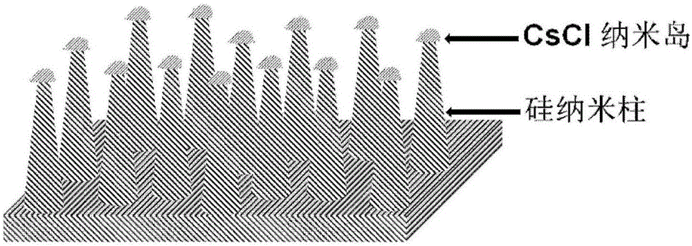
[0038] The invention provides a heterojunction solar cell with a large aspect ratio silicon nano column array as a substrate and a preparation method thereof. This type of heterojunction solar cell is based on a P-type silicon nano-pillar array with a large aspect ratio, and an N-type thin film material is wrapped on the surface of the nano-pillar array to form a heterojunction. The manufacturing method includes: first, prepare a large aspect ratio nano-pillar array on the surface of the P-type silicon wafer; then prepare an aluminum back field on the back; then, use magnetron sputtering to wrap zinc oxide on the surface of the silicon nano-pillar array. N-type material layer such as cadmium sulfide; in the next step, a transparent conductive layer of ITO is covered on the surface of the N-type material layer; finally, a titanium silver electrode is prepared on the upper surface.

[0039] The present invention proposes to apply the self-assembly technology of cesium chloride nano...

Embodiment example

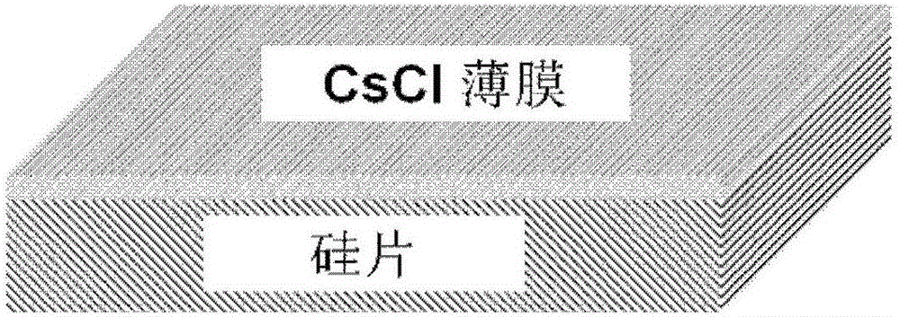
[0049] Step 1: The silicon wafer is selected as P-type doped, single-sided polishing, Crystal orientation, thickness is 400 microns, resistivity is 1-5 ohm. The cesium chloride film was prepared by thermal evaporation method on the polished surface with a thickness of 200 nanometers.

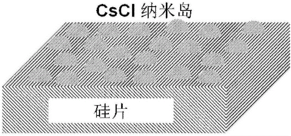
[0050] Step 2: Put the silicon wafer plated with cesium chloride film in step 1 into a ventilated chamber with a humidity of 40%. The humidity is controlled by the flow of moist gas flowing into the chamber. Development is carried out for 30 minutes under this humidity condition. The cesium chloride film agglomerates into a nano-island structure, forming a cesium chloride nano-island structure on the surface of the silicon wafer. The average diameter of cesium chloride nano islands is 400 nanometers.

[0051] Step 3: Put the silicon wafer with the cesium chloride island structure on the surface in step 2 into the etching chamber of the plasma etching machine, the etching process parameters are pres...


PUM

PropertyMeasurementUnit
diameteraaaaaaaaaa
heightaaaaaaaaaa
thicknessaaaaaaaaaa

Abstract

The invention discloses a heterojunction solar cell taking a silicon nanorod array as a substrate and a fabrication method of the heterojunction solar cell. The solar cell uses a silicon nanorod array with a large depth-width ratio as the substrate, and other thin film materials are wrapped by a magnetron sputtering method to form a heterojunction structure. The fabrication method comprises the following steps of fabricating the silicon nanorod array with the large depth-width ratio on a surface of a P-type silicon wafer by a self-assembly method of a cesium chloride nanometer island; fabricating an aluminum back filed on a back surface; wrapping a surface of the silicon nanorod array with an N-type material layer such as zinc oxide and cadmium sulfide by the magnetron sputtering method; covering a surface of the N-type material layer with an ITO transparent conductive layer; and fabricating a titanium-silver electrode on an upper surface. The solar cell taking the silicon nanorod array with the large depth-width ratio as the substrate has the advantages that 1, the surface ratio of the substrate can be effectively increased, the effective area of a heterojunction is expanded, and absorption to incident light is improved; and 2, by means of a favorable light trapping effect, reflection can be reduced, and the performance of the heterojunction cell is improved.

Description

Technical field [0001] The invention relates to semiconductor micro-nano processing technology and the technical field of heterojunction solar cells, in particular to a heterojunction solar cell with a large aspect ratio silicon nano-pillar array as a substrate and a preparation method thereof. Background technique [0002] Nano-array is a new type of surface structure, which has huge industrial applications in many fields such as solar cells and LEDs. Nano-texturing has the characteristic of reducing visible light reflection. For traditional monocrystalline or polycrystalline silicon solar cells, nano-texturing such as nanowires and nanopillars can be directly prepared on the silicon surface, and the light trapping effect of the nanoarray can effectively improve the short-circuit current and battery efficiency of the solar cell. [0003] The cumbersome preparation process and high cost limit the promotion of traditional solar cells. Using a simple process to deposit a layer of tr...

Claims


Application Information

Patent Timeline
Patent Type & Authority Applications(China)
IPC IPC(8): H01L31/0264H01L31/028H01L31/074H01L31/18
CPCH01L31/0264H01L31/028H01L31/074H01L31/1804Y02E10/547Y02P70/50
Inventor 刘静伊福廷王波张天冲王雨婷
Owner INST OF HIGH ENERGY PHYSICS CHINESE ACAD OF SCI
Why Eureka
Try Eureka