Resistive material-based micro electron source and array thereof and implementation method

An implementation method and technology of electron source, applied in electronic science and field, can solve the problems of small emission current, low emission efficiency and high working voltage, and achieve the effects of low working voltage and temperature, good emission performance and convenient processing

Inactive Publication Date: 2016-12-21
PEKING UNIV
View PDF5 Cites 10 Cited by
  • Summary
  • Abstract
  • Description
  • Claims
  • Application Information

AI Technical Summary

Problems solved by technology

However, due to the complex structure of the micro field emission electron source, the high electric field intensity required for field emission, the strong dependence of the field emission performance on the atomic structure of the emission tip, and the instability of the tip atomic structure under strong fields, the micro field emission electron source has a micro Disadvantages such as complex processing technology, high working voltage, uncontrollable emission performance, poor array uniformity, and ultra-high vacuum required for work
These shortcomings greatly limit the application of miniature field emission electron sou...

Method used


Image

  • Resistive material-based micro electron source and array thereof and implementation method
  • Resistive material-based micro electron source and array thereof and implementation method
  • Resistive material-based micro electron source and array thereof and implementation method

Examples


Embodiment 1

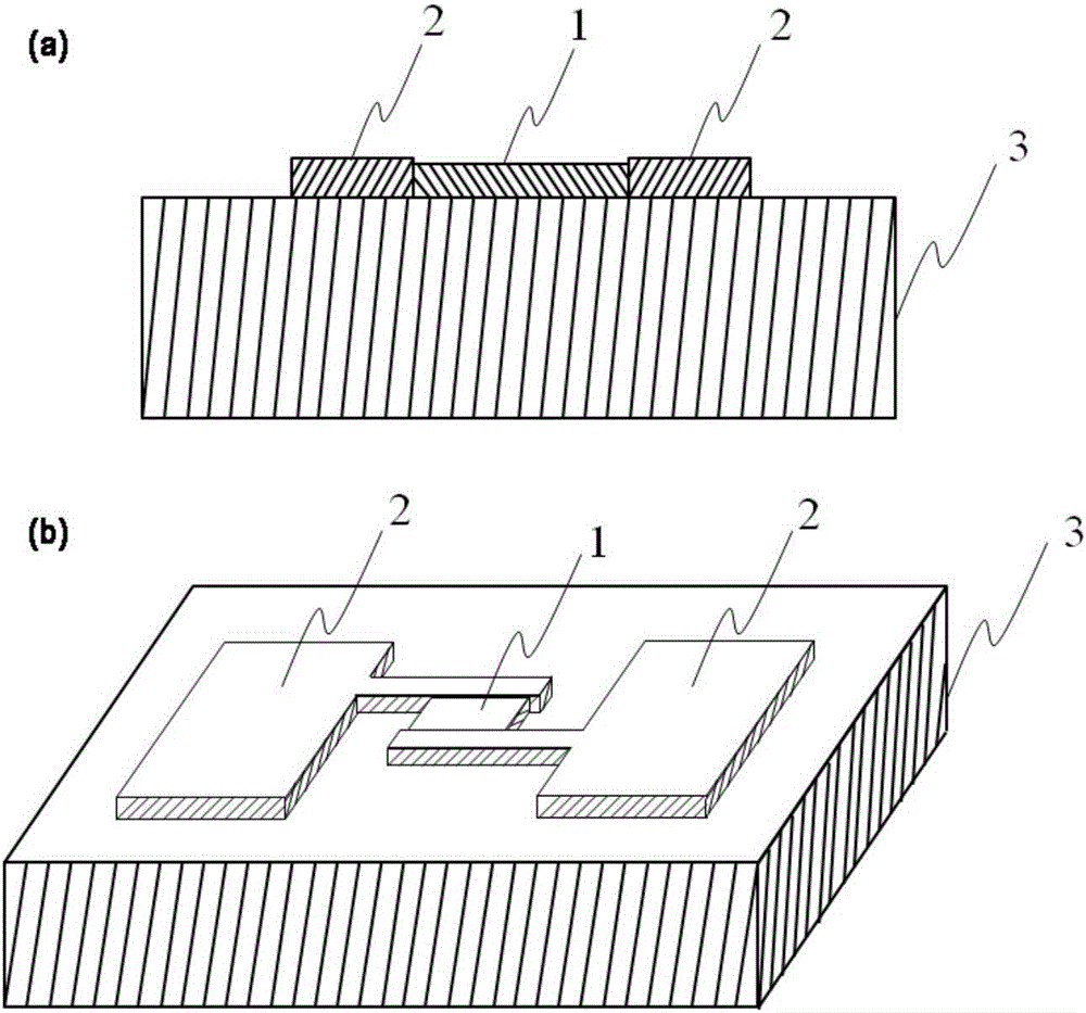
[0034] In this embodiment, the resistive material unit and the electrode pair are located at the same height as the substrate surface, and the resistive material unit is located between the electrode pair.

[0035] Such as figure 1 As shown, the micro-electron source constructed in this embodiment includes: a resistive material unit 1, an electrode pair 2 for activating the resistive material unit and driving its electron emission, and a lining for supporting the resistive material unit and the electrode pair. Bottom 3.

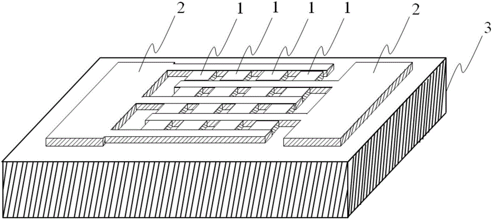
[0036] Such as figure 2 As shown, the micro-electron source array constructed in this embodiment includes: 4×4 figure 1 In the resistive material unit 1 of the miniature electron source shown, all the miniature electron sources are arranged on the same substrate 3 and connected in parallel through the interdigitated electrode pairs 2 .

[0037] The electrode pair in this embodiment includes two parts: the part directly connected with the resistive materia...

Embodiment 2

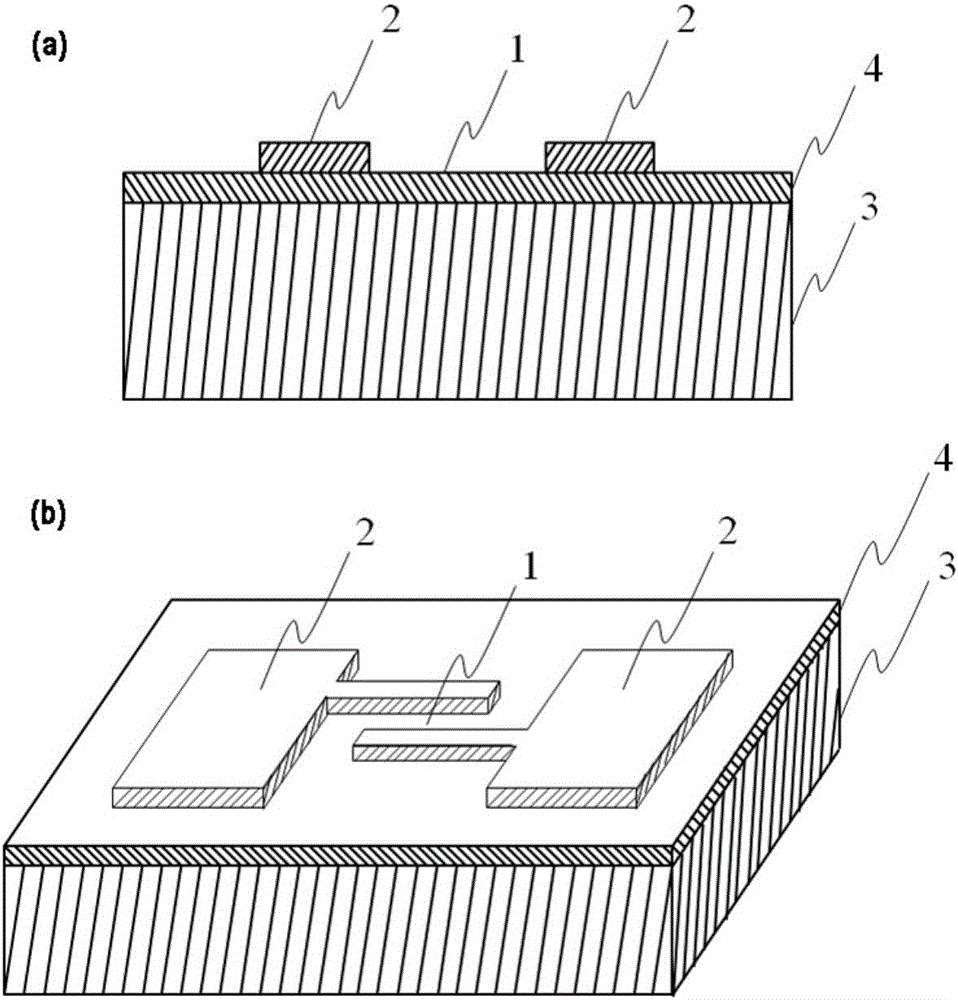
[0039]In this embodiment, the surface of the substrate is covered with a resistive material film, the electrode pairs are located above the resistive material film, and the resistive material film between the electrode pairs constitutes a resistive material unit

[0040] Such as image 3 As shown, the micro-electron source constructed in this embodiment includes: a support substrate 3, a resistive material film 4 covering the surface of the substrate, an electrode pair 2, and a resistive switch composed of a resistive material film between the electrode pairs 2. Materials Unit 1.

[0041] Such as Figure 4 As shown, the micro electron source array constructed in this embodiment includes: 2×4 image 3 In the resistive material unit 1 of the miniature electron source shown, all the miniature electron sources are arranged on the same substrate 3 and connected in parallel through the interdigitated electrode pairs 2 .

[0042] The electrode pair in this embodiment includes two ...

Embodiment 3

[0045] Next, using the method of micromachining, using palladium and titanium as electrodes, and silicon oxide as the resistive material, the micro-electron source in Example 2 is realized on the surface of the silicon substrate. The specific steps are as follows:

[0046] (1) Place the silicon wafer in a reaction tube made of quartz glass, heat the reaction tube to 900° C. and feed oxygen to oxidize the surface of the silicon wafer to obtain a 300 nm thick silicon oxide film.

[0047] (2) After spin-coating electron beam photoresist PMMA, electron beam exposure, developing and fixing, electron beam evaporation coating, stripping and other process steps, titanium palladium metal (0.5nm titanium / 70nm palladium) electrode pair, the minimum width of the prepared metal electrode is 220nm, and the electrode pair spacing is 50nm.

[0048] (3) Set one electrode of the above-prepared electrode pair to zero potential, and the other electrode to negative potential, gradually increase...


PUM


Abstract

The invention discloses a resistive material-based micro electron source and an array thereof and an implementation method. The micro electron source comprises a resistive material unit and an electrode pair connected with the resistive material unit, wherein the electrode pair is used for driving the resistive material unit to emit electrons. A certain number of micro electron sources are arranged on a same substrate to form the array of the micro electron source. The micro electron source and the array thereof disclosed by the invention have the characteristics of being simple in structure, convenient to process, low in working voltage and temperature, good in emission performance and the like, and can be widely used for various electronic devices relating to the electron source.

Description

technical field [0001] The invention belongs to the field of electronic science and technology, and in particular relates to a micro-electron source based on a resistive material, a micro-electron source array and a realization method thereof. Background technique [0002] The electron source is considered to be the heart of vacuum electronic devices (such as X-ray tubes, high-power microwave tubes, cathode ray tubes, etc.), providing the latter with the free electron beams necessary for their work, and therefore is an essential key to vacuum electronic devices element. At present, almost all practical vacuum electronic devices use thermal emission electron sources. Since the thermal emission electron source heats the electron emitter to a high temperature (generally greater than 1000K) so that the electrons inside the emitter obtain enough kinetic energy to be emitted across the surface barrier, it has the advantages of high operating temperature, large power consumption, ...

Claims


Application Information

Patent Timeline
IPC IPC(8): H01J1/304H01J9/02
CPCH01J9/18H01J37/073H01J3/022H01J9/025H01J9/027H01J23/04H01J29/028H01J35/065H01J2237/06341H01J1/304H01J1/312H01J1/316H01J2201/30449H01J2201/30461
Inventor 魏贤龙吴功涛
Owner PEKING UNIV
Why Eureka
Try Eureka