High-specific-surface-area boron-doped diamond electrode and preparation method and application thereof

A diamond electrode, high specific surface area technology, applied in the direction of electrodes, chemical instruments and methods, electrolysis process, etc., can solve the problems of electrodes restricting the mass transfer efficiency of the electrode surface, etc., to improve sewage treatment efficiency, improve current efficiency, and increase conductivity and the effect of electrocatalytic performance

Active Publication Date: 2017-02-22
NANJING DAIMONTE TECH CO LTD
View PDF8 Cites 84 Cited by
  • Summary
  • Abstract
  • Description
  • Claims
  • Application Information

AI Technical Summary

Problems solved by technology

[0003]The traditional flat electrode is a two-dimensional electrode, its real electrode area is similar to the apparent electrode area, and the low specific surface area of ​​the electrode seriously restricts the mass transfer efficiency of the electrode surface

Method used


Image

  • High-specific-surface-area boron-doped diamond electrode and preparation method and application thereof
  • High-specific-surface-area boron-doped diamond electrode and preparation method and application thereof
  • High-specific-surface-area boron-doped diamond electrode and preparation method and application thereof

Examples


Embodiment 1

[0072] Embodiment 1: flat type (board)

[0073] (1) cleaning the flat niobium substrate;

[0074] (2) adopting the magnetron sputtering method to deposit a layer of metal chromium layer with a thickness of 500nm on the flat niobium surface;

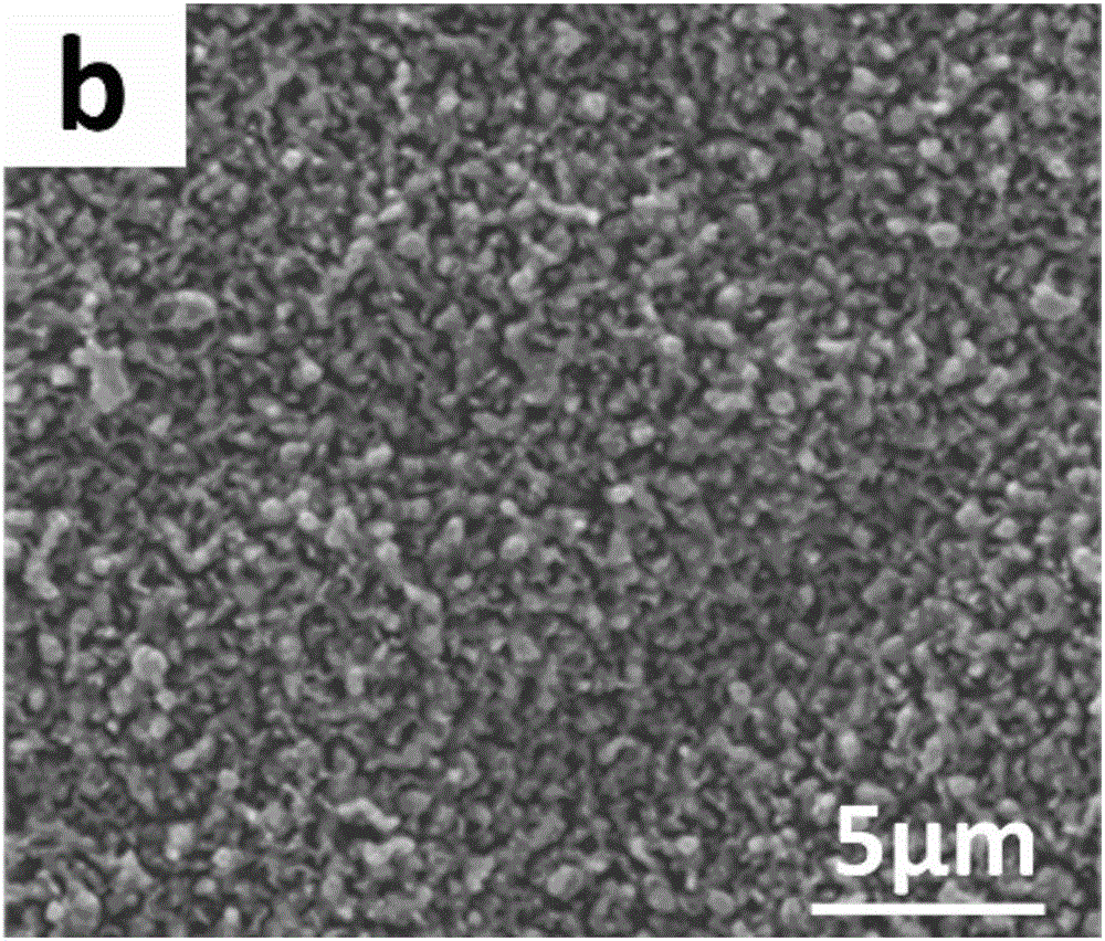
[0075] (3) Place the chromium-modified flat niobium in the suspension of nanocrystalline and microcrystalline diamond mixed particles, vibrate in ultrasonic for 30 minutes, and disperse evenly to obtain a niobium matrix with nanocrystalline and microcrystalline diamond particles adsorbed on the surface .

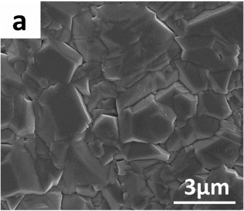
[0076] (4) Boron-doped diamond film is deposited by hot wire CVD, deposition process parameters: hot wire distance 6mm, deposition temperature 700-750°C, hot wire temperature 2200°C, deposition pressure 3KPa, gas ratio (CH 4 :H 2 :B 2 h 6 ) (sccm) is 3:97:0.3, obtains diamond film thickness 20 μ m by controlling deposition time;

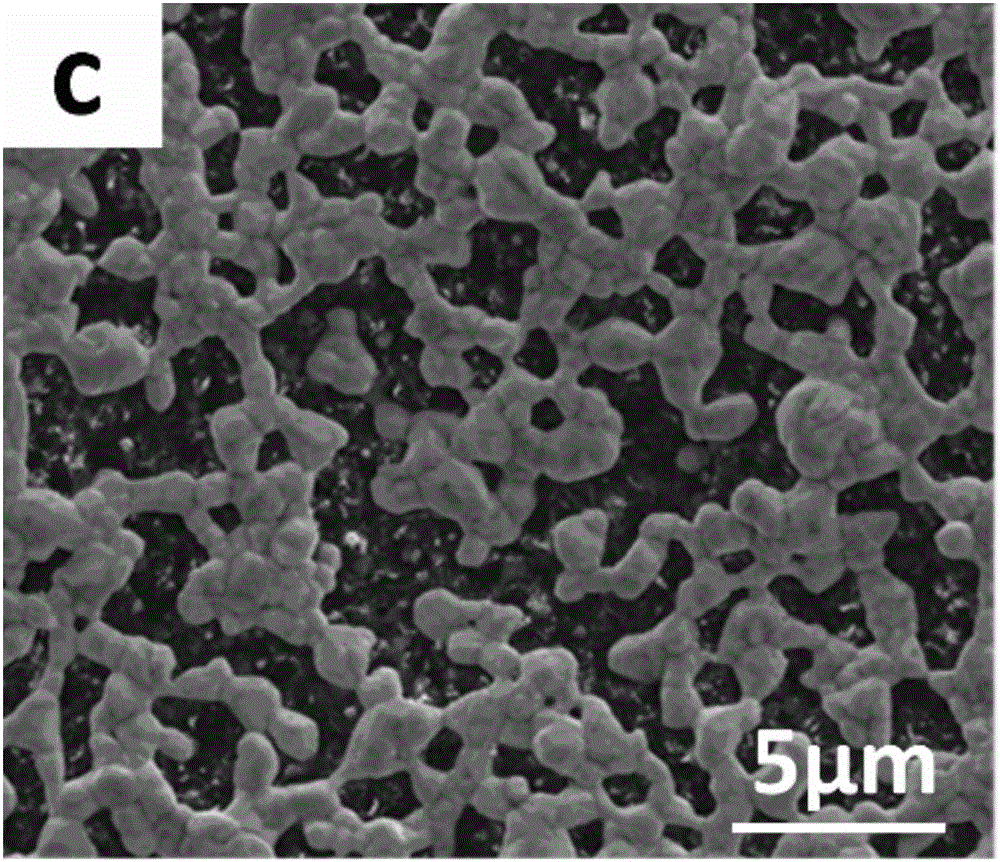
[0077] (5) The boron-doped diamond surface prepared in step (4) adopts the magnetron sputtering depos...

Embodiment 2

[0081] Embodiment 2: flat type (board)

[0082] (1) cleaning the tungsten sheet;

[0083] (2) Place the tungsten sheet in a suspension of mixed particles of nanocrystalline and microcrystalline diamond, oscillate in an ultrasonic wave for 30 minutes, and disperse evenly to obtain a niobium matrix with nanocrystalline and microcrystalline diamond particles adsorbed on the surface.

[0084] (3) Boron-doped diamond film was deposited by hot wire CVD, deposition process parameters: hot wire distance 6mm, deposition temperature 700-750°C, hot wire temperature 2200°C, deposition pressure 3KPa, gas ratio (CH 4 :H 2 :B 2 h 6 ) (sccm) is 3:97:0.3, obtains diamond film thickness 25 μ m by controlling deposition time;

[0085] (4) The boron-doped diamond surface prepared in step (3) adopts the magnetron sputtering deposition method to deposit a metal nickel layer, and the specific sputtering parameters are sputtering current 400mA, argon flow 10sccm, sputtering pressure 0.4Pa, sputte...

Embodiment 3

[0089] Embodiment 3: flat type (board)

[0090] (1) silicon wafer is cleaned;

[0091] (2) Place the silicon chip in a suspension of mixed particles of nanocrystalline and microcrystalline diamond, vibrate in an ultrasonic wave for 30 minutes, and disperse evenly to obtain a niobium substrate with nanocrystalline and microcrystalline diamond particles adsorbed on the surface.

[0092] (3) Boron-doped diamond film was deposited by hot wire CVD, deposition process parameters: hot wire distance 6mm, deposition temperature 700-750°C, hot wire temperature 2200°C, deposition pressure 3KPa, gas ratio (CH 4 :H 2 :B 2 h 6 )(sccm) is 3:97:0.3, deposition time 4h;

[0093] (4) The boron-doped diamond surface prepared in step (3) adopts the magnetron sputtering deposition method to deposit a metal nickel layer, and the specific sputtering parameters are sputtering current 400mA, argon flow 10sccm, sputtering pressure 0.4Pa, sputtering Time 60s;

[0094] (5) Put the sample obtained i...


PUM

PropertyMeasurementUnit
thicknessaaaaaaaaaa
sizeaaaaaaaaaa
thicknessaaaaaaaaaa

Abstract

The invention discloses a high-specific-surface-area boron-doped diamond (BDD) electrode which comprises an electrode substrate. A boron-doped diamond layer is arranged on the surface of the electrode substrate. Or, a transition layer is arranged on the surface of the substrate, and then a boron-doped diamond layer is arranged on the surface of the transition layer. Metal particles are distributed in the diamond layer, and tiny holes and / or pointed cones are distributed on the surface of the diamond layer. Compared with a traditional plate electrode, the boron-doped diamond electrode contains a large number of tiny holes and pointed cones and has the extremely high specific surface area, and the large current intensity is provided through the low current intensity; and meanwhile, due to the different electrode configurations of the substrate and modification of surface graphene and / or carbon nano tubs (CNT), the mass transfer process can be greatly improved, the current efficiency and the electrochemical property are greatly improved, and the BDD electrode with high electrocatalytic activity and high using efficiency is prepared. The electrode can be widely applied in the fields of electrochemical wastewater purification treatment, electrochemical biosensors, strong oxidant electrochemical synthesis, electrochemical detection and the like.

Description

technical field [0001] The invention discloses a boron-doped diamond electrode with a high specific surface area, a preparation method and application thereof, and belongs to the technical field of electrode preparation. Background technique [0002] Diamond film electrode is a material with excellent physical and chemical properties. Its high mechanical strength, excellent chemical stability and electrochemical performance, and the surface of the electrode will not change significantly under high-intensity current loads. It has broad prospects in electrochemical applications. During the growth of the diamond film, boron is doped to make the prepared boron-doped diamond film into a semiconductor or a conductor with metallic properties, which is obtained by depositing it on the surface of some electrode substrates such as titanium sheets, silicon sheets, graphite, etc. Boron-doped diamond electrodes are the focus of sewage purification treatment, electrochemical biosensors a...

Claims


Application Information

Patent Timeline
Patent Type & Authority Applications(China)
IPC IPC(8): C23C16/02C23C16/27C23C16/56C25B11/04G01N27/26C02F1/461C02F101/30
CPCC02F1/46109C02F2001/46147C02F2101/30C23C16/0272C23C16/0281C23C16/277C23C16/278C23C16/56C25B11/091G01N27/26
Inventor 魏秋平周科朝马莉张龙余志明
Owner NANJING DAIMONTE TECH CO LTD
Why Eureka
Try Eureka