Preparation of methylamine lead-iodine nanowire under air environment and application of photoelectric detector

An air environment, methylamine lead iodine technology, which is applied to the preparation of methylamine lead iodine nanowires in an air environment and the application field of photodetectors, can solve problems such as performance to be improved, and achieve the effect of improving photoelectric performance.

Inactive Publication Date: 2017-04-26
HEBEI UNIV OF TECH
View PDF12 Cites 13 Cited by
  • Summary
  • Abstract
  • Description
  • Claims
  • Application Information

AI Technical Summary

Problems solved by technology

At present, the application of perovskite structure nanowires in photoelectric performance is less, and its performance needs to be improved. One of the ways to improve its performance is to prepare pure-phase single-crystal methylamine-lead-iodine nanowires. Therefore, the preparation process is simple and convenient in the air environment. Methylamine lead iodide nanowires with controllable size and shape are imperative

Method used


Image

  • Preparation of methylamine lead-iodine nanowire under air environment and application of photoelectric detector
  • Preparation of methylamine lead-iodine nanowire under air environment and application of photoelectric detector
  • Preparation of methylamine lead-iodine nanowire under air environment and application of photoelectric detector

Examples


Embodiment 1

[0024] Example 1: Pure phase MAPbI 3 The specific preparation process of nanowires.

[0025] Dissolve 0.227 g of lead iodide in 2 ml of DMF solution at room temperature to prepare a lead iodide precursor solution with a concentration of 0.3 mmol / ml.

[0026] Dissolve 17.5mg of MAI in 5ml of IPA solution to form a 17.5mg / 5ml solution of MAI and IPA.

[0027] After taking 5 μl of DMF solution and 200ul of 17.5mg / 5ml MAI and IPA solution with a pipette, mix the two solutions to obtain a mixed solution.

[0028] Use a pipette to take 20μl of 0.3mmol / ml lead iodide precursor solution, drop it on the clean glass base, place it on a spin coater, let it stand for 10s, and spread it evenly at a low speed of 2000r / 5s, then 6000r / The film was formed at a high speed of 5s without any heat treatment, and immediately spin-coated with 5μl of DMF and 200μl of MAI and IPA mixed solution at a speed of 4000r / 20s, and then heat-treated at 100°C to obtain MAPbI 3 Nanowires.
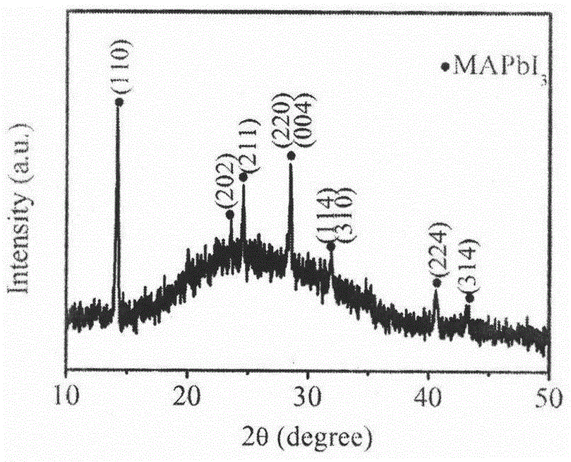
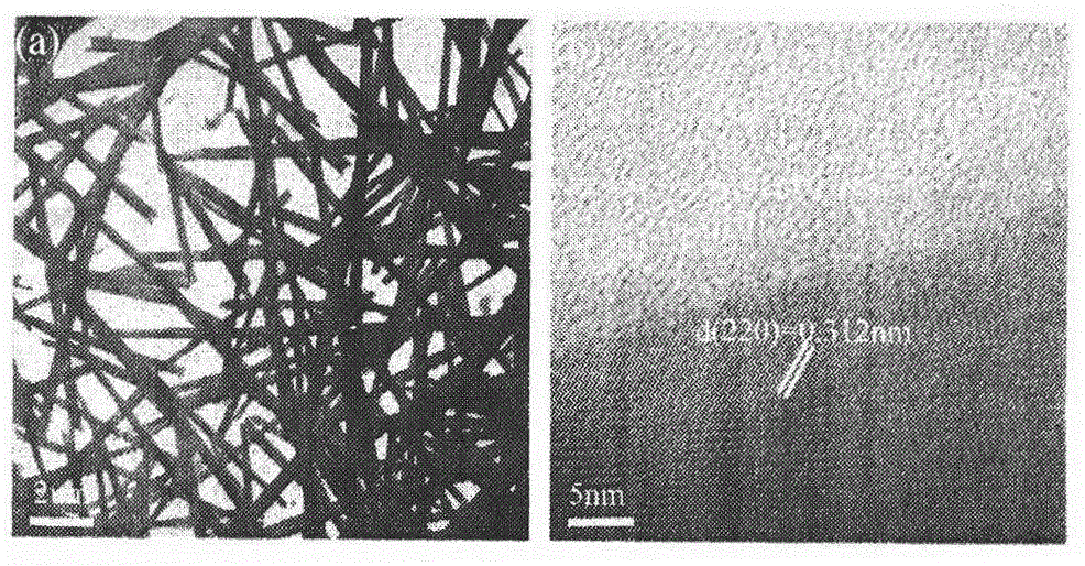
[0029] figure 1...

Embodiment 2

[0031] Example 2: MAPbI 3 The specific preparation process of nanowire morphology and size control.

[0032] The difference between this embodiment and Example 1 is that the concentration of lead iodide is different, respectively 0.1848g, 0.227g, 0.3696g and 0.462g of lead iodide are dissolved in 2ml of DMF solution at room temperature, the concentration is respectively 0.2mmol / ml , 0.3mmol / ml, 0.4mmol / ml and 0.5mmol / ml of lead iodide precursor prepared MAPbI 3 Nanowires.

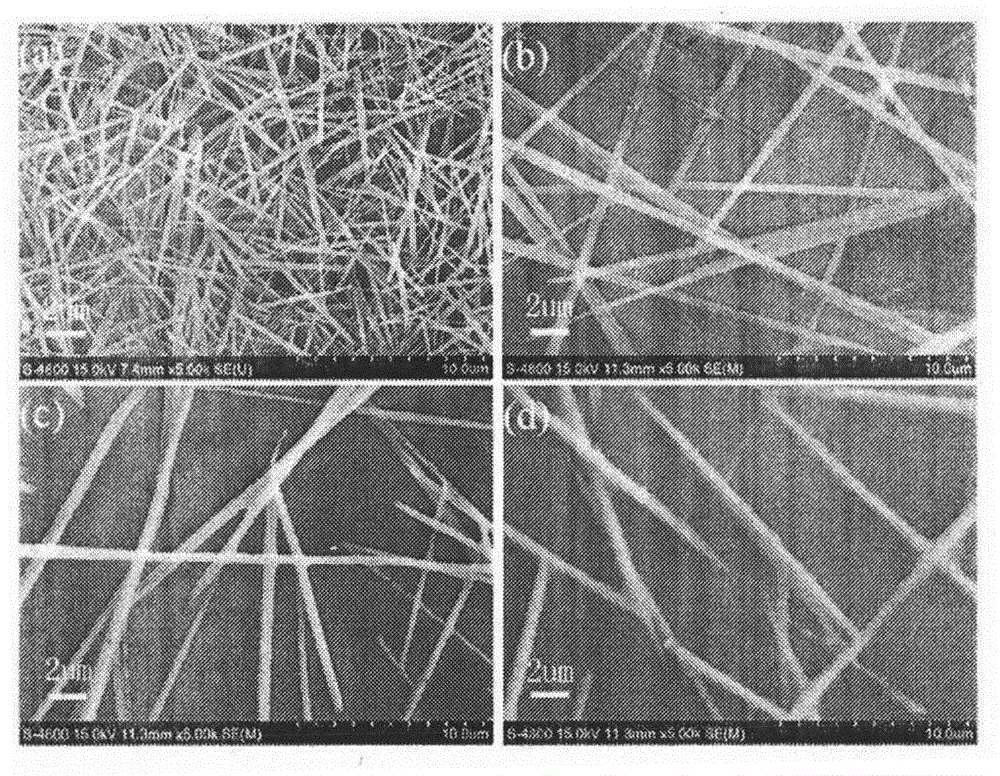
[0033] image 3 MAPbI prepared for different concentrations of lead iodide solutions 3 SEM images of nanowires. Figures (a), (b), (c) and (d) lead iodide concentrations are 0.2mmol / ml, 0.3mmol / ml, 0.4mmol / ml and 0.5mmol / ml respectively. It can be seen from the figure that with the change of the concentration of the lead iodide precursor, the prepared MAPbI 3The size and shape of the nanowires also changed. The nanowires at low lead iodide concentrations were slightly sparser, the length of the nanowir...

Embodiment 3

[0035] Example 3: MAPbI of different sizes and shapes 3 Fabrication process of nanowires for photodetector applications.

[0036] The difference between embodiment 3 and embodiment 2 is that the MAPbI with a concentration of 0.2mmol / ml, 0.3mmol / ml, 0.4mmol / ml and 0.5mmol / ml 3 The nanowires are grown on the cleaned interdigitated electrode substrate, and the probes with positive and negative electrodes are contacted with a pair of electrodes on the interdigitated electrodes, and the output current changes with time according to the voltage of 0.1V applied to both ends of the electrodes. Relational diagram, get I-T diagram of photoresponse.

[0037] Figure 5 MAPbI prepared for lead iodide solutions at different concentrations 3 Photoelectric response I-T diagram of nanowires. Figures (a), (b), (c) and (d) lead iodide concentrations are 0.2mmol / ml, 0.3mmol / ml, 0.4mmol / ml and 0.5mmol / ml in turn. From the figure, we can see that when the concentration of lead iodide is reduce...


PUM

PropertyMeasurementUnit
lengthaaaaaaaaaa
diameteraaaaaaaaaa

Abstract

The invention discloses preparation of a methylamine lead-iodine nanowire with a perovskite structure and control of a size and a shape. The pure-phase methylamine lead-iodine nanowire is successfully prepared; a growth key factor of the methylamine lead-iodine nanowire is the amount of DMF (Dimethyl Formamide) and the DMF has the effect of dissolving lead iodide; and the dissolved lead iodide and methylamine iodine react rapidly to crystallize, nucleate and grow, so as to form a one-dimensional nanowire. The method comprises the steps of dissolving and recrystallizing. The invention further discloses combination of the methylamine lead-iodine nanowire and a photoelectric detector, wherein growth is carried out on a pure SiO2 substrate, and the methylamine lead-iodine nanowire has good photoelectric properties; and the methylamine lead-iodine nanowire grows on a carbon-containing supported net membrane at a temperature of 100 DEG C, and types of crystals of the nanowire are tested.

Description

technical field [0001] The invention belongs to the preparation of perovskite structure organic-inorganic metal halide nanometer material and its application in photoelectric performance. Background technique [0002] With the development of society, energy issues have gradually become a concern of people. People use a large amount of fossil energy to cause serious air pollution, and the energy storage of fossil energy is very limited. issue concerned. [0003] The new perovskite structure organic-inorganic metal halide methylamine lead iodide is due to its excellent photovoltaic properties, such as direct band gap, suitable band gap, high light absorption coefficient, high electron and hole mobility, long Carrier diffusion length, etc., has become a hot research topic in the field of photovoltaic research. [0004] At present, compared with the traditional three-dimensional structure, the one-dimensional structure has superior carrier transport characteristics, which can ...

Claims


Application Information

Patent Timeline
Patent Type & Authority Applications(China)
IPC IPC(8): C07C211/04C07C209/00H01L51/42H01L51/46H01L51/48B82Y30/00B82Y40/00
CPCB82Y30/00B82Y40/00C07C209/00C07C211/04H10K71/12H10K85/30H10K30/10Y02E10/549Y02P70/50
Inventor 张新刘辉刘彩池郝秋艳任刚
Owner HEBEI UNIV OF TECH
Why Eureka
Try Eureka