Surface-mounted super capacitor and preparation method thereof
A supercapacitor, chip technology, applied in the field of electrochemistry, can solve the problems of difficult breakthrough in the structure design of chip devices, and achieve the effects of low cost, low environmental pollution, degradability, etc.
- Summary
- Abstract
- Description
- Claims
- Application Information
AI Technical Summary
Problems solved by technology
Method used
Image
Examples
preparation example Construction
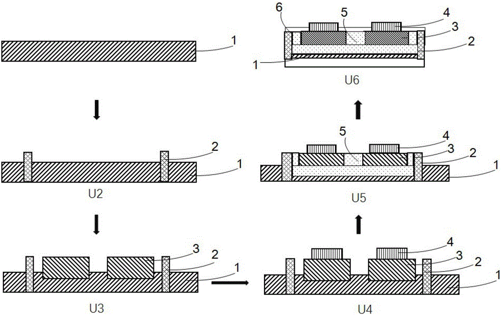
[0024] Such as figure 1 Shown, is the flow chart of the preparation method of the patch type supercapacitor of this specific embodiment, comprises the following steps:
[0025] U1, prepare the active material slurry.
[0026] The above-mentioned active material slurry is used for subsequent formation of electrodes. The active material slurry can be prepared by mixing the active material with the conductive agent and the binder, adding an organic solvent, and stirring thoroughly. By controlling the different proportions of various materials, the conductivity and rheological properties of the slurry can be changed. Preferably, the active material slurry is prepared by mass ratio of 60%-90% active material, 5%-30% conductive agent and 5%-10% binder, adding an appropriate amount of solvent and stirring uniformly for 2-6 hours. By applying the formula to supercapacitors, the electrode active materials can be better played.
[0027] In the above active material slurry, the activ...
Embodiment 1
[0052] 1. Mix the active material slurry according to the mass ratio of active material, binder, and conductive material at 8:1:1, add solvent N-methylpyrrolidone, and stir for 4 hours. The active material is activated carbon slurry; the binder is polyvinylidene fluoride; the conductive agent is conductive carbon black.
[0053] 2. Select cellulose paper with a thickness of 35 μm as the substrate 1, epoxy resin as the high-temperature resistant resin, and infiltrate the epoxy resin on the substrate by screen printing to form several pieces with an area of 32×25mm 2 The frame cofferdam 2 is placed in an oven until the resin is cured, and the frame line width of the frame cofferdam is controlled within 300 μm.
[0054] 3. Based on the orifice printing process, the active material slurry is printed in the cofferdam 2 of the paper substrate 1, and the area of each electrode material 3 formed is 12×20mm 2 , the distance between two pieces of electrode material 3 is 0.4 mm. Af...
Embodiment 2
[0062] The specific preparation process is the same as in Example 1, except that the active material replaces the active carbon slurry in Example 1 with a mixture of carbon nanotubes and molybdenum disulfide, and the binder replaces the polyvinylidene fluoride in Example 1 with polyvinyl alcohol. Ethylene, conductive agent replaces the conductive carbon black in embodiment 1 with acetylene black.
[0063] In this embodiment, the composition of the electrode material is adjusted relative to the embodiment 1, and the rest of the processes are the same. After verification, the volt-ampere scan diagram, constant current charge-discharge curve diagram and the voltammeter scan diagram before and after enduring high-temperature reflow soldering of the supercapacitor made are the same as those in Example 1. Figure 4~6 similar and will not be listed here.
PUM
 Abstract
Description
Claims
Application Information


