Mixed light interconnection system based on standard CMOS (Complementary Metal-Oxide-Semiconductor Transistor) process

An interconnection system and mixed light technology, which is applied in the direction of electrical components, circuits, semiconductor devices, etc., can solve the problems of weak detection performance of Si-based LEDs and inability to realize two-way communication, so as to reduce light transmission distance, reduce electrical interference, and avoid The effect of crosstalk

Inactive Publication Date: 2017-05-10
TIANJIN UNIV
View PDF4 Cites 6 Cited by
  • Summary
  • Abstract
  • Description
  • Claims
  • Application Information

AI Technical Summary

Problems solved by technology

However, there is only a thin layer of gate oxide between the LED and the detector, and the influence of the isolation electrical effect and thermal effect is not good; secondly, the monocrystalline silicon LED in the lower layer can only be used as a light-emitting device, polysilicon can only be used as a receiving device and cannot realize two-way communication; Three Si-based LEDs emit infrared light with forward-biased carrier injection. Although reverse-biased breakdown emits visible light, the wavelength of light is also around 700nm. Due to the thin polysilicon layer, it has a negative impact on the long-wavelength light emitted by Si-based LEDs. The detection performance is weak, while the single crystal silicon deep junction is relatively good at detecting long-wavelength light

Method used


Image

  • Mixed light interconnection system based on standard CMOS (Complementary Metal-Oxide-Semiconductor Transistor) process
  • Mixed light interconnection system based on standard CMOS (Complementary Metal-Oxide-Semiconductor Transistor) process
  • Mixed light interconnection system based on standard CMOS (Complementary Metal-Oxide-Semiconductor Transistor) process

Examples


Embodiment Construction

[0028] A hybrid optical interconnection system based on a standard CMOS process of the present invention will be described in detail below with reference to embodiments and drawings.

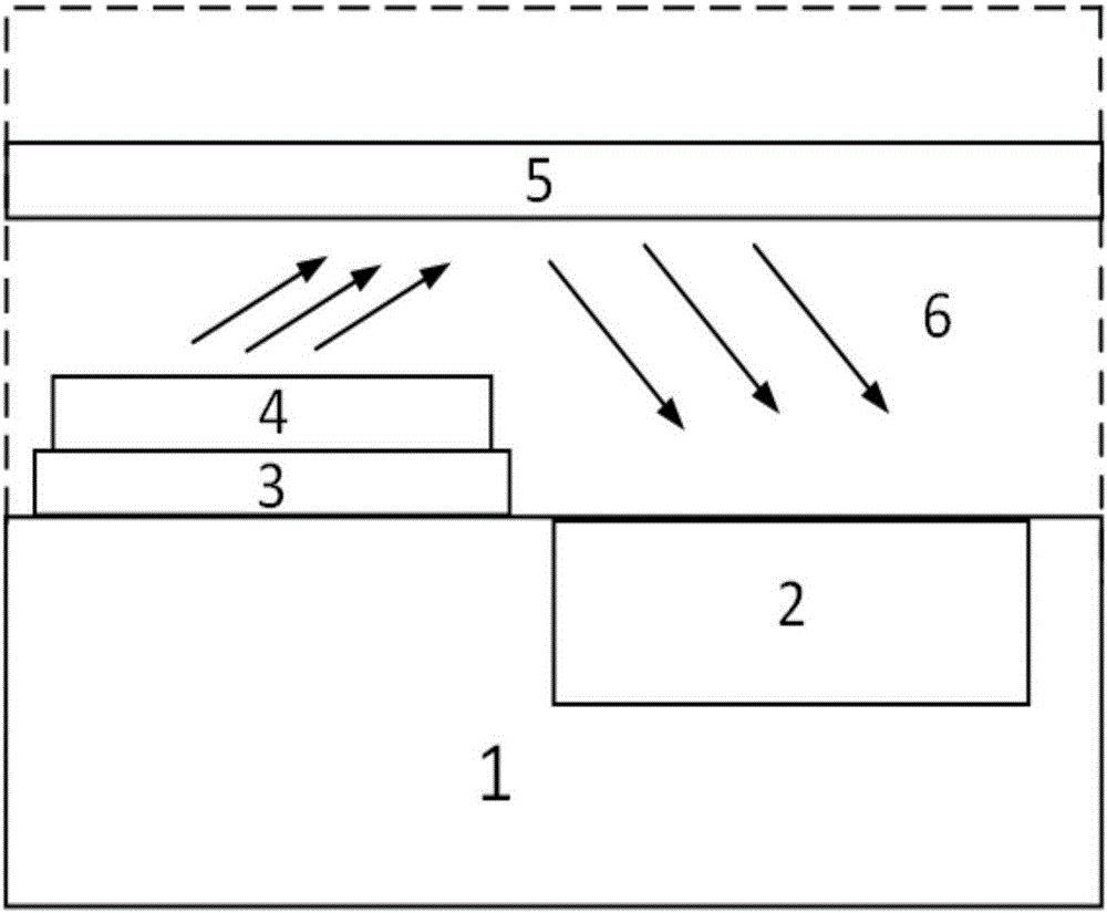
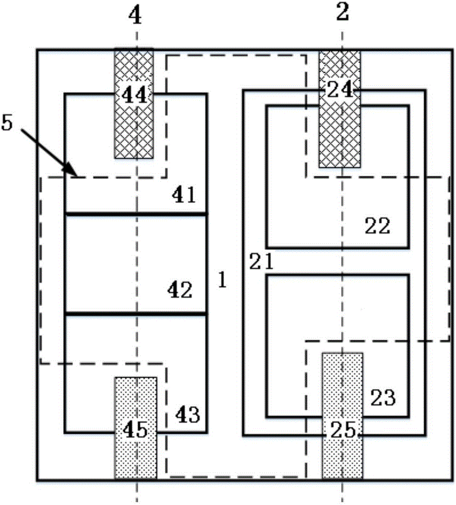
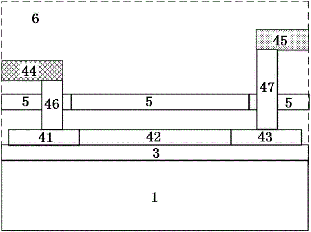
[0029] A hybrid optical interconnection system based on a standard CMOS process of the present invention includes a polysilicon LED, an optical waveguide, a single crystal silicon detector composed of a P+ / N well, and a P-type substrate; the polysilicon LED includes a polysilicon LED anode and its The contact area, the polysilicon LED cathode and its contact area, and the i area of ​​the polysilicon LED; the polysilicon LED can emit infrared light with forward bias, and can also emit visible light with reverse bias. The waveguide is metal and its underlying SiO 2 layer; the monocrystalline silicon photodetector includes a monocrystalline silicon detector anode and its contact, a monocrystalline silicon detector cathode and its contact, and an N well in a P-type substrate; the photodetector is re...


PUM


Abstract

The invention discloses a mixed light interconnection system based on a standard CMOS (Complementary Metal-Oxide-Semiconductor Transistor) process. The system comprises a substrate, a silicon dioxide body is arranged on the upper surface of the substrate, a metal layer for reflecting light is arranged at the upper part in the silicon dioxide body, a gate oxide layer achieving an isolating effect and a polycrystalline silicon LED (Light Emitting Diode) for emitting light are sequentially arranged in the silicon dioxide body and on the upper surface of the substrate from bottom to top, and a monocrystalline silicon PD for receiving light reflected from the metal layer is arranged close to the upper surface in the substrate and located on one side of the gate oxide layer and the polycrystalline silicon LED. The system can convert input electrical signals into light signals by light emission of the polycrystalline silicon LED, then the light signals are reflected by the metal and converted into electrical signals by a monocrystalline silicon photoelectric detector, and the converted electrical signals are output. The system can effectively shorten the light transmission distance while realizing light transmission on chip without increasing the manufacturing cost of an integrated circuit, and reduces the electrical interference.

Description

technical field [0001] The present invention relates to a hybrid optical interconnection system. In particular, it relates to a hybrid optical interconnection system based on a standard CMOS process consisting of a monocrystalline silicon photodetector (PD) and a polycrystalline silicon light emitting diode (LED). Background technique [0002] With the rapid development of science and technology, the feature size of integrated circuits is becoming smaller and smaller, and the integration level of chips is also becoming higher and higher under the guidance of Moore's Law. Microelectronics products are developing in the direction of small and precise. . In the 21st century, the development of microelectronics has encountered the bottleneck of physical limits. Further scaling down through "Moore's Law" would not only dramatically increase manufacturing costs, but also lead to undesired physical effects. Another more pressing bottleneck is the delay and power consumption of e...

Claims


Application Information

Patent Timeline
Patent Type & Authority Applications(China)
IPC IPC(8): H01L31/173
CPCH01L31/173
Inventor 毛陆虹丛佳谢生肖谧郭维廉
Owner TIANJIN UNIV
Why Eureka
Try Eureka