

A Group III Nitride Semiconductor Avalanche Photodiode Detector
A nitride semiconductor and avalanche photoelectric technology, applied in the field of detectors, can solve the problems of difficult manufacturing process, reduce device filling factor, etc., and achieve the effects of reducing surface leakage current, preventing edge breakdown, and enhancing electric field strength
- Summary
- Abstract
- Description
- Claims
- Application Information
AI Technical Summary
Problems solved by technology
Method used
Image

Examples
Embodiment Construction
[0019] The present invention will be described in detail below in conjunction with the accompanying drawings.
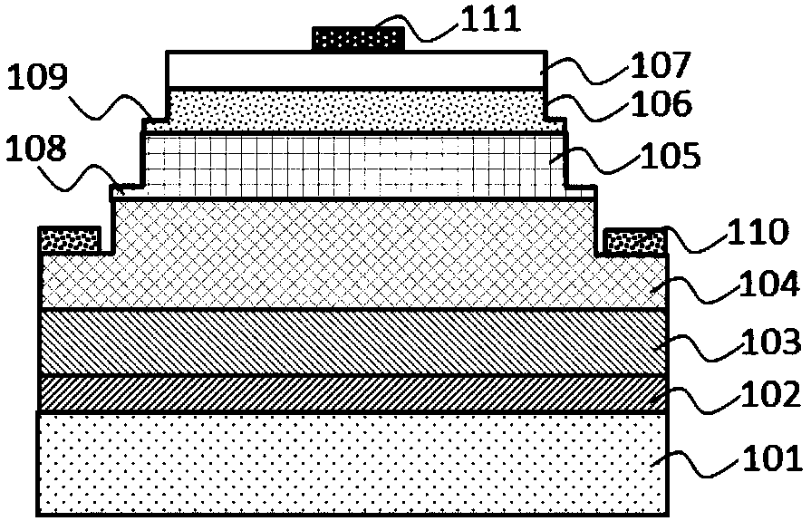
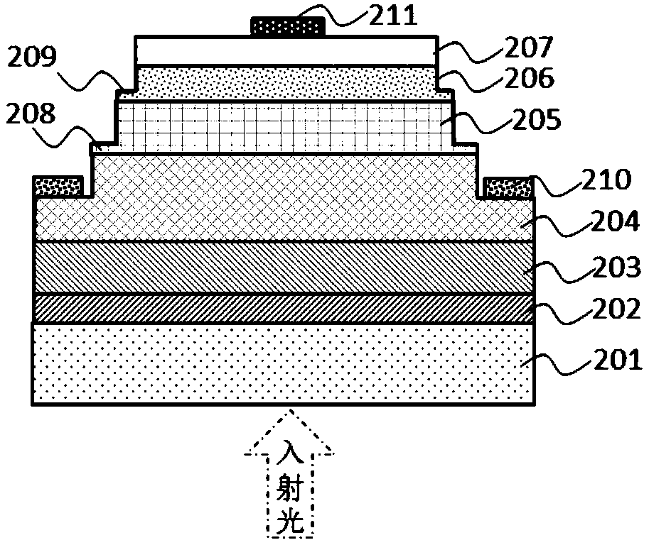
[0020] This example figure 2, a group III nitride AlGaN-based avalanche photodetector is shown in the figure. The device adopts the method of incident light signal from the substrate side, including: a sapphire substrate 201 and a low-temperature AlN buffer layer grown sequentially on the substrate. 202, high temperature AlN transition layer 203, heavily doped n-type Al 0.55 Ga 0.45 N ohmic contact layer 204, non-uniformly doped with p-type Al 0.4 Ga 0.6 N active layer 205, p-type doped Al 0.4 Ga 0.6 N layer 206, heavily doped p-type Al 0.4 Ga 0.6 N ohmic electrode contact layer 207, the step 208 on the edge of the active layer 205 formed by etching, the step 209 on the edge of the p-type doped layer 206 formed by etching, and the step 209 formed on the n-type Al 0.4 Ga 0.6 Ohmic contact electrode 210 on N layer 204, making p-type Al 0.4 Ga 0.6 Ohmic cont...
PUM
 Abstract
Description
Claims
Application Information