Application of hybridization perovskite nanometer material in preparing all-optical spinning electron device
A nanomaterial, perovskite technology, applied in the fields of instruments, optics, nonlinear optics, etc., can solve the problems of high preparation cost, high device preparation cost, slow switching speed of all-optical switches, etc., to reduce the preparation cost and preparation process. Simple, fast switching effects
- Summary
- Abstract
- Description
- Claims
- Application Information
AI Technical Summary
Problems solved by technology
Method used
Image

Examples
Embodiment Construction
[0029] It should be pointed out that the following detailed description is exemplary and intended to provide further explanation to the present application. Unless defined otherwise, all technical and scientific terms used herein have the same meaning as commonly understood by one of ordinary skill in the art to which this application belongs.
[0030] It should be noted that the terminology used here is only for describing specific implementations, and is not intended to limit the exemplary implementations according to the present application. As used herein, singular forms are intended to include plural forms unless the context clearly dictates otherwise. In addition, it should also be understood that when the terms "comprising" and / or "comprises" are used in this specification, it indicates the presence of features, steps, operations, means, components and / or their combination.
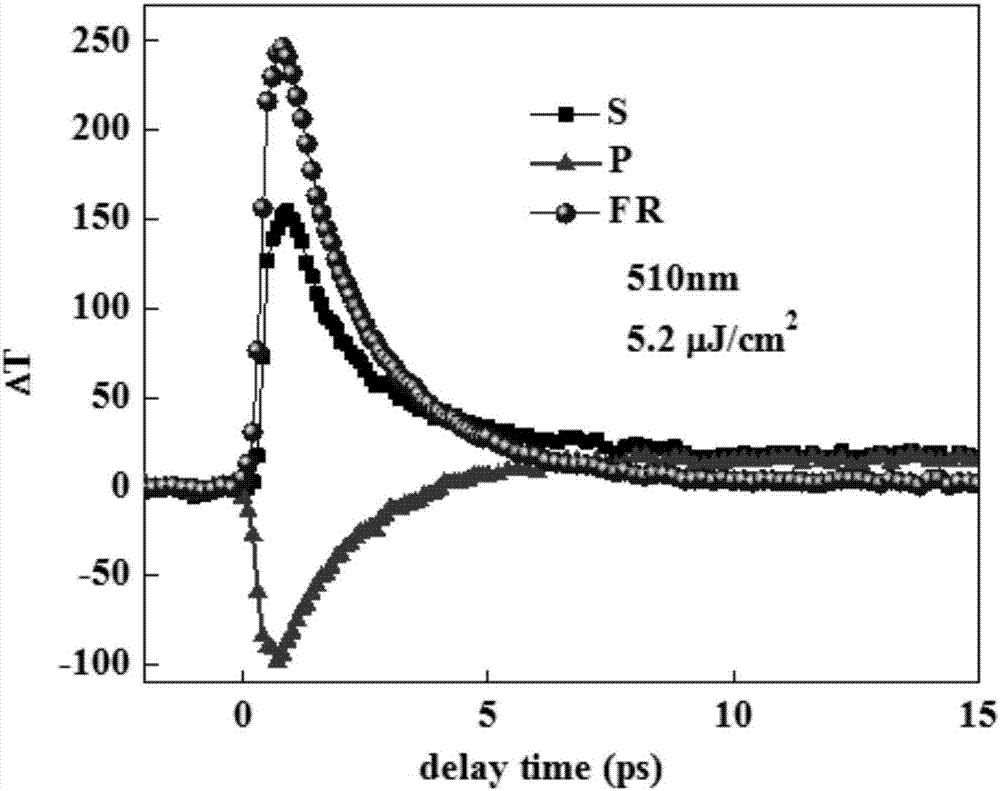
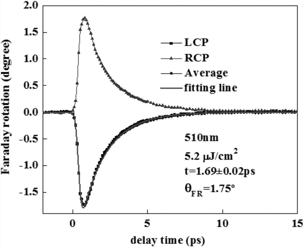
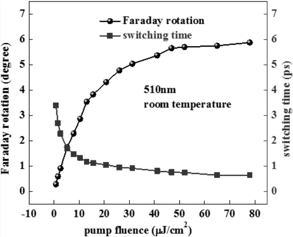
[0031] We measured CH using the femtosecond time-resolved optomagnetic Faraday effect 3 NH 3...
PUM
| Property | Measurement | Unit |
|---|---|---|
| Thickness | aaaaa | aaaaa |
Abstract
Description
Claims
Application Information
 - Generate Ideas
- Intellectual Property
- Life Sciences
- Materials
- Tech Scout
- Unparalleled Data Quality
- Higher Quality Content
- 60% Fewer Hallucinations
Browse by: Latest US Patents, China's latest patents, Technical Efficacy Thesaurus, Application Domain, Technology Topic, Popular Technical Reports.
© 2025 PatSnap. All rights reserved.Legal|Privacy policy|Modern Slavery Act Transparency Statement|Sitemap|About US| Contact US: help@patsnap.com