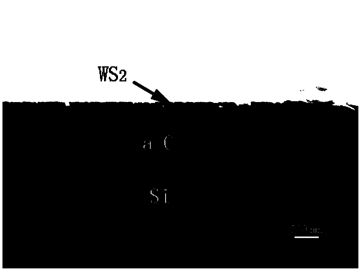
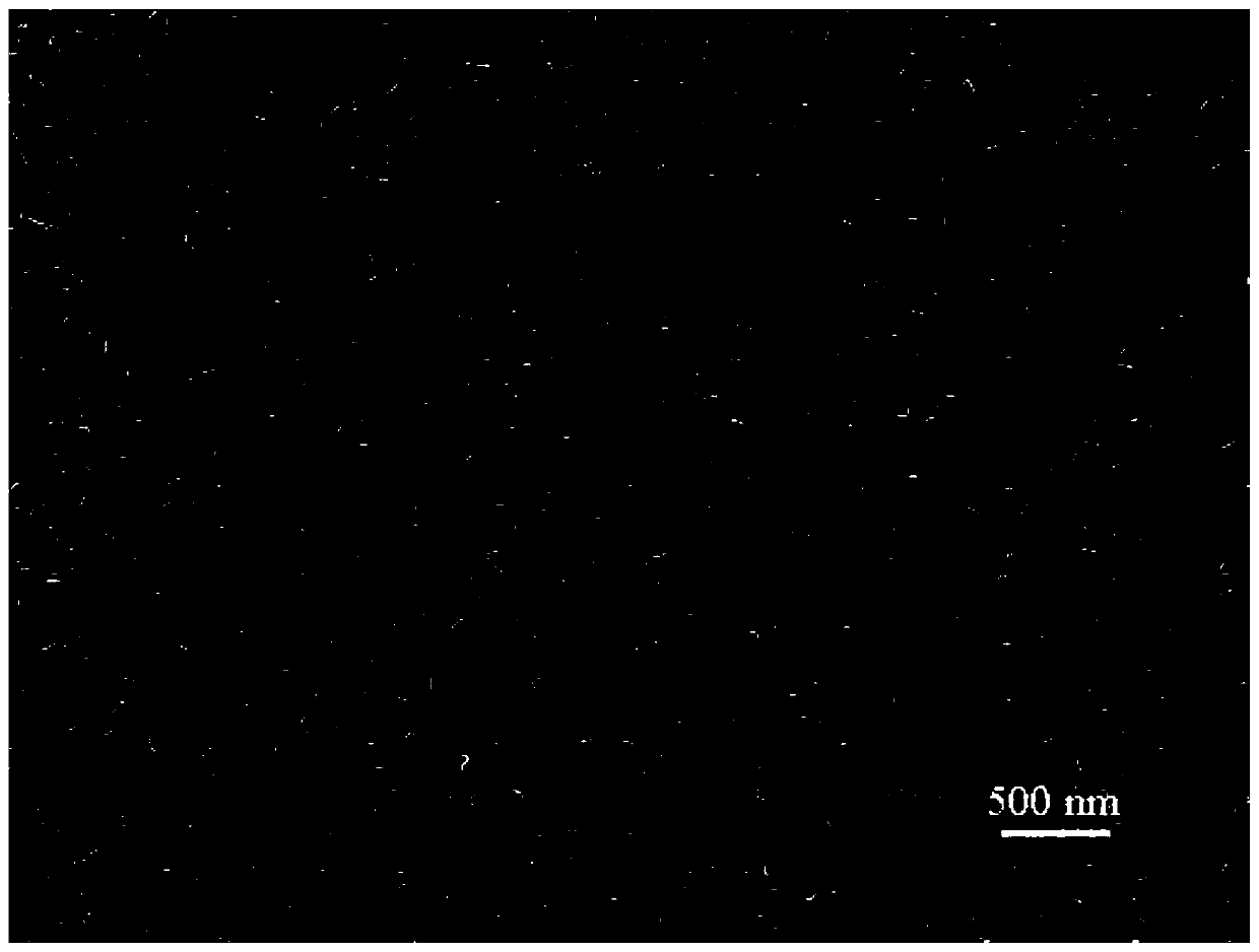
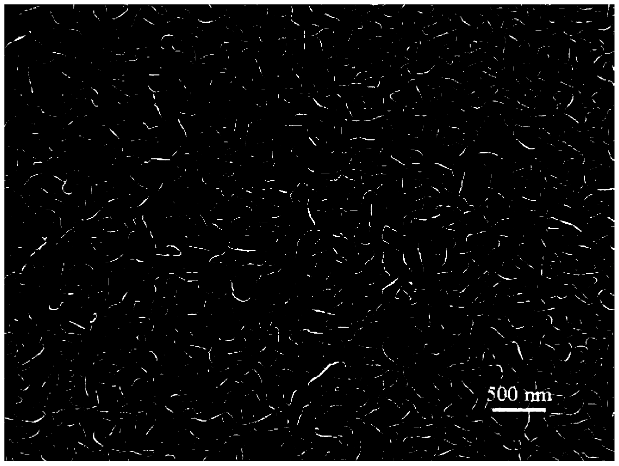
A kind of preparation method of wear-resistant tungsten disulfide film
A technology of tungsten disulfide and thin film, which is applied in metal material coating process, vacuum evaporation plating, coating, etc., can solve the problems of limited improvement of wear resistance, large increase of friction coefficient, high process cost, etc., and achieve reduction The effect of protection level, large elastic modulus and simple process
- Summary
- Abstract
- Description
- Claims
- Application Information
AI Technical Summary
Problems solved by technology
Method used
Image
Examples
Embodiment 1
[0029] (1) Preparation before coating
[0030] Take a single crystal polished silicon wafer ( or crystal orientation) with a size of 20×20×0.45mm, degrease it by ultrasonic degreasing with absolute alcohol, soak in 10% (volume fraction) hydrofluoric acid solution, deionize After washing with water, dry with hot air and set aside. Take Φ60×3mm graphite target (99.99% carbon mass fraction) and WS 2 Each piece of target (WS 2 Mass fraction 99.9%), put into the multi-target magnetron sputtering chamber together with the substrate, and vacuumize the deposition chamber to 1.0×10 -3 Pa, adjust the distance between the target and the base to 70mm, adjust the pulse DC bias power supply, so that the output amplitude of the negative bias voltage is 50V, and the duty cycle is 50%.
[0031] (2) Carbon film deposition
[0032] Introduce high-purity argon gas (flow rate 50 sccm) and stabilize the air pressure at 0.2 Pa, start heating the substrate and keep the temperature constant at 30...
Embodiment 2
[0036] (1) Preparation before coating
[0037] Same as Example 1.
[0038] (2) Carbon film deposition
[0039] Introduce high-purity argon gas (flow rate 50 sccm) and stabilize the air pressure at 0.6 Pa, start heating the substrate and keep the temperature constant at 200 ° C, turn on the graphite target sputtering power supply for sputtering (power is 65 W), and the duration is 270 min. The thickness of the carbon film is about 370nm.
[0040] (3)WS 2 thin film deposition
[0041] Keep the substrate temperature at 200°C and the deposition pressure at 0.6Pa, and turn on the WS 2 Target sputtering power supply for sputtering (power is 60W), duration is 9min, the obtained WS 2 The film thickness is about 140nm.
Embodiment 3
[0043] (1) Preparation before coating
[0044] Same as Example 1.
[0045] (2) Carbon film deposition
[0046] Introduce high-purity argon gas (flow rate 50 sccm) and stabilize the air pressure at 0.8 Pa, start heating the substrate and keep the temperature constant at 100 ° C, turn on the graphite target sputtering power supply for sputtering (power is 80 W), the duration is 118 min, and the obtained The thickness of the carbon film is about 210nm.
[0047] (3)WS 2 thin film deposition
[0048] Increase the heating temperature of the substrate and keep it at 200°C, adjust the deposition pressure to 0.6Pa, and turn on the WS 2 Target sputtering power supply for sputtering (power is 60W), duration is 33min, the obtained WS 2 The film thickness is about 515nm.
PUM
| Property | Measurement | Unit |
|---|---|---|
| thickness | aaaaa | aaaaa |
| thickness | aaaaa | aaaaa |
| thickness | aaaaa | aaaaa |
Abstract
Description
Claims
Application Information


