Method and product for loading semiconductor photocatalyst on surface of electrospun fiber

A photocatalyst and surface loading technology, applied in the field of nanomaterials, can solve the problems of small impact on the specific surface area of ​​composite materials, small photocatalyst loading, and difficulty in large-scale production, and achieve separation and recycling, reusable, low cost, and fiber diameter. small effect

Active Publication Date: 2017-08-29
QINGDAO UNIV
View PDF5 Cites 19 Cited by
  • Summary
  • Abstract
  • Description
  • Claims
  • Application Information

AI Technical Summary

Problems solved by technology

At present, the commonly used carrier materials for loading titanium dioxide include glass, graphene, carbon fiber and some polymer materials. However, when these materials support photocatalysts, the photocatalyst loading capacity is small and the specific surface area of ​​the composite material is small, which affects the photocatalytic efficiency, or the cost is relatively high. high, complex preparation methods and difficult mass production, etc. In addition, these composite photocatalytic materials are mostly rigid materials, which cannot adapt to the application environment that needs to change shape, and are easy to damage

Method used


Image

  • Method and product for loading semiconductor photocatalyst on surface of electrospun fiber
  • Method and product for loading semiconductor photocatalyst on surface of electrospun fiber
  • Method and product for loading semiconductor photocatalyst on surface of electrospun fiber

Examples


Embodiment 1

[0030] A method for loading a semiconductor photocatalyst on the surface of an electrospun fiber, comprising the following steps:

[0031] (1) Electrospinning template fiber material: Add polyvinylidene fluoride powder to a mixed solvent composed of dimethylformamide (DMF) and acetone and stir in a water bath at 40°C to obtain an electrospinning precursor solution. The mass ratio of dimethylformamide (DMF) and acetone is 1:1, and the mass percent of polyvinylidene fluoride contained in the electrospinning precursor solution is 20%; prepare flexible micro-nano by electrospinning Fibrous membrane, the spinning voltage is 9 kV, the spinning distance is 11 cm, the collector pole of the electrospinning device used is the drum collector pole, and the polyvinylidene fluoride nanofiber membrane is obtained as the template fiber material on the collector pole, and the obtained The template material is cut into small square pieces of 1.5 cm x 1.5 cm and set aside;

[0032](2) Prepare t...

Embodiment 2

[0038] A method for loading a semiconductor photocatalyst on the surface of an electrospun fiber, comprising the following steps:

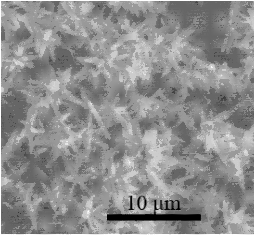
[0039] (1) Electrospinning template fiber material: Add TPU into a mixed solvent composed of DMF and THF, and magnetically stir for 2 hours to obtain an electrospinning precursor solution. The mass ratio of DMF and THF in the mixed solvent is 1:1, The mass percentage of TPU contained in the electrospinning precursor solution is 12%; the flexible micro-nano fiber membrane is prepared by electrospinning, the spinning voltage is 12 kV, and the spinning distance is 15 cm. Obtain TPU fiber membrane (morphology such as image 3 As shown, the magnification is 1000 times) as the template fiber material, the resulting template material is cut into square pieces of 1.5 cm × 1.5 cm, and set aside;

[0040] (2) Prepare the reaction solution: under normal temperature conditions, weigh 75ml of deionized water and Zn(NO 3 )·6H 2 O 3.5 g was added to the conta...

Embodiment 3

[0044] A method for loading a semiconductor photocatalyst on the surface of an electrospun fiber, comprising the following steps:

[0045] (1) Electrospinning template fiber material: polyacrylonitrile PAN was added to DMF, and magnetically stirred for 2 hours to obtain an electrospinning precursor solution. The mass percentage of PAN contained in the electrospinning precursor solution was 12%; The flexible micro-nano fiber membrane was prepared by electrospinning, the spinning voltage was 15 kV, and the spinning distance was 10 cm. The PAN fiber membrane was obtained on the collector as the template fiber material, and the resulting template material was cut into 1.5 cm × 1.5 cm square pieces, set aside;

[0046] (2) Prepare the reaction solution: under normal temperature conditions, weigh 15 ml of deionized water and 15 ml of hydrochloric acid solution into the container, then add 1 ml of butyl titanate while stirring, and continue stirring for 20 minutes to obtain a hydroth...


PUM


Abstract

The invention discloses a method and product for loading a semiconductor photocatalyst on the surface of an electrospun fiber. The method comprises the following steps: (1) preparing an electrospinning template fiber material; (2) preparing a reaction solution for synthesizing the semiconductor photocatalyst through a hydro-thermal method; (3) soaking the template fiber material obtained in the step (1) in the reaction solution obtained in the step (2), putting the reaction solution with the template fiber material in a closed hydro-thermal kettle to perform a hydro-thermal reaction, and synthesizing a nano semiconductor photocatalyst on a fiber surface of the template fiber material through the hydro-thermal method; and (4) performing cleaning and drying. The method is easy to operate, and can realize large-scale production, and an obtained product is a flexible material which is difficult to damage and high in photocatalytic efficiency, can be separated and recovered easily after use, and can be reused.

Description

technical field [0001] The invention belongs to the technical field of nanometer materials, and in particular relates to a method and a product for loading a semiconductor photocatalyst on the surface of an electrospun fiber. Background technique [0002] Photocatalytic technology is a new type of green environmental protection technology. Semiconductor photocatalysts include titanium dioxide (TiO 2 ), zinc oxide (ZnO), tin oxide (SnO 2 ), zirconium dioxide (ZrO 2 ), cadmium sulfide (CdS) and other oxides and sulfide semiconductors, among which titanium dioxide has become the most popular nano photocatalyst material in the world because of its strong oxidation ability, stable chemical properties and non-toxicity. Semiconductor photocatalyst photocatalytic technology has attractive application prospects in the fields of hydrogen production from water and sewage treatment. However, the existing commercial semiconductor photocatalysts, such as titanium dioxide photocatalysts...

Claims


Application Information

Patent Timeline
Patent Type & Authority Applications(China)
IPC IPC(8): B01J31/38B01J31/26B01J35/06
CPCB01J31/26B01J31/38B01J35/004B01J35/065
Inventor 龙云泽张志广张俊刘慧张斌王晓雄闫旭
Owner QINGDAO UNIV
Why Eureka
Try Eureka