

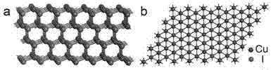
Cuprous iodide two-dimensional material, and preparation and application thereof
A cuprous iodide, two-dimensional material technology, applied in the field of nanomaterials, can solve the problems of uneven morphology, poor crystallinity, thick nanosheets, etc., and achieve the effects of good morphology, good crystallinity, and regular morphology
- Summary
- Abstract
- Description
- Claims
- Application Information
AI Technical Summary
Problems solved by technology
Method used
Image

Examples
Embodiment 1
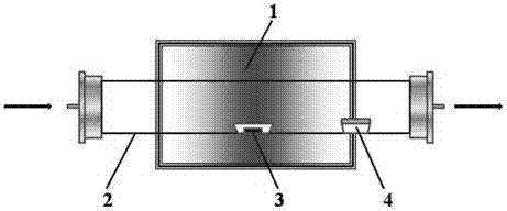
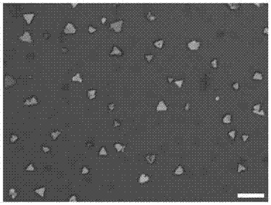
[0076] Preparation of cuprous iodide nanosheets: Add 0.5 g of cuprous iodide powder into a small porcelain boat, and then put it into the constant temperature zone of a horizontal quartz tube with a diameter of one inch. With a small piece of Si / 300nmSiO 2The silicon oxide sheet is used as the growth substrate of the nanosheet, placed in another porcelain boat, and placed in the variable temperature zone downstream of the furnace to obtain an appropriate crystal growth temperature. Before growing, the quartz tube is first flushed with argon to remove oxygen and water vapor. Then the furnace is rapidly raised to 360°C, and the argon gas flow rate is adjusted to 225 sccm, and the temperature is kept constant for 35 minutes. A single crystal cuprous iodide nanosheet will be formed on the silicon wafer position 9em away from the source. The experimental device for preparing cuprous iodide nanosheets is shown in Fig. figure 2 As shown (the color in the furnace is red and gradual...
Embodiment 2
[0079] Preparation of cuprous iodide nanosheets: Add 0.5 g of cuprous iodide powder into a small porcelain boat, and then put it into the constant temperature zone of a horizontal quartz tube with a diameter of one inch. With a small piece of Si / 300nmSiO 2 The silicon oxide sheet is used as the growth substrate of the nanosheet, placed in another porcelain boat, and placed in the variable temperature zone downstream of the furnace to obtain an appropriate crystal growth temperature. Before growing, the quartz tube is first flushed with argon to remove oxygen and water vapor. Then the furnace is rapidly raised to 390°C, and the argon gas flow rate is adjusted to 225 sccm, and the temperature is kept constant for 10 minutes, and single crystal cuprous iodide nanosheets will be formed at the position of the silicon wafer 9 cm away from the source. The experimental device for preparing cuprous iodide nanosheets is shown in Fig. figure 2 As shown (the color in the furnace is red...
Embodiment 3
[0082] Preparation of cuprous iodide nanosheets: Add 0.5 g of cuprous iodide powder into a small porcelain boat, and then put it into the constant temperature zone of a horizontal quartz tube with a diameter of one inch. With a small piece of Si / 300nmSiO 2 The silicon oxide sheet is used as the growth substrate of the nanosheet, placed in another porcelain boat, and placed in the variable temperature zone downstream of the furnace to obtain an appropriate crystal growth temperature. Before growing, the quartz tube is first flushed with argon to remove oxygen and water vapor. Then the furnace was quickly raised to 410°C, and the argon gas flow rate was adjusted to 200 sccm, and the temperature was kept constant for 20 minutes. A single-crystal cuprous iodide nanosheet would be formed at the position of the silicon wafer at a distance of 8 em from the source. The experimental device for preparing cuprous iodide nanosheets is shown in Fig. figure 2 As shown, the optical photog...
PUM
| Property | Measurement | Unit |
|---|---|---|
| Thickness | aaaaa | aaaaa |
| Thickness | aaaaa | aaaaa |
| Thickness | aaaaa | aaaaa |
Abstract
Description
Claims
Application Information