GaN-based light-emitting diode epitaxial slice and growth method thereof
A light-emitting diode, gallium nitride-based technology, applied in electrical components, circuits, semiconductor devices, etc., can solve problems such as reduced internal quantum efficiency, lattice defects, and dislocations that are difficult to eliminate, so as to reduce defects and improve crystal quality. , Improve the effect of internal quantum efficiency and antistatic ability
- Summary
- Abstract
- Description
- Claims
- Application Information
AI Technical Summary
Problems solved by technology
Method used
Image
Examples
Embodiment 1
[0028] An embodiment of the present invention provides a GaN-based light-emitting diode epitaxial wafer, figure 1 It is a structural schematic diagram of an epitaxial wafer of a gallium nitride-based light-emitting diode provided by the present invention, such as figure 1 As shown, the gallium nitride-based light-emitting diode epitaxial wafer includes a substrate 1 and a low-temperature buffer layer 2 covering the substrate 1, a high-temperature buffer layer 3, an undoped GaN layer 4, an N-type layer 5, and an MQW light-emitting layer 6. and P-type layer 7 . Wherein, the high-temperature buffer layer 3 is a lamination structure in which undoped InGaN layers and magnesium-doped InGaN layers are grown alternately, the number of undoped InGaN layers is n, and the number of magnesium-doped InGaN layers is n-1, where n> 2 and n is an integer.
[0029] By doping magnesium in the high-temperature buffer layer, the high-temperature buffer layer is mainly in a three-dimensional grow...
Embodiment 2
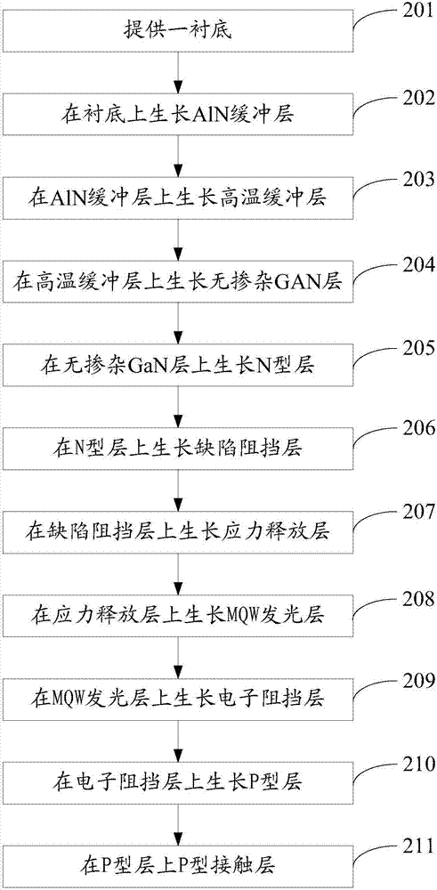
[0044] An embodiment of the present invention provides a method for growing a gallium nitride-based light-emitting diode epitaxial wafer, figure 2 It is a flowchart of a method for growing an epitaxial wafer of a gallium nitride-based light-emitting diode provided by the present invention, such as figure 2 As shown, the growth method is suitable for growing the GaN-based light-emitting diode epitaxial wafer provided in Embodiment 1 of the present invention, and the method includes:
[0045] Step 201, providing a substrate.
[0046] Specifically, the substrate may be a sapphire substrate, or a Si substrate or a SiC substrate.
[0047] Step 202, growing an AlN buffer layer on the substrate.
[0048]Specifically, the AlN buffer layer is prepared in PVD (Physical Vapor Deposition, physical vapor deposition) equipment, and the preparation conditions are not limited, and the AlN buffer layer with a thickness of 10-35 nm is grown.
[0049] Step 203, growing a high-temperature bu...
PUM
| Property | Measurement | Unit |
|---|---|---|
| Thickness | aaaaa | aaaaa |
| Growth temperature | aaaaa | aaaaa |
| Thickness | aaaaa | aaaaa |
Abstract
Description
Claims
Application Information
 - R&D Engineer
- R&D Manager
- IP Professional
- Industry Leading Data Capabilities
- Powerful AI technology
- Patent DNA Extraction
Browse by: Latest US Patents, China's latest patents, Technical Efficacy Thesaurus, Application Domain, Technology Topic, Popular Technical Reports.
© 2024 PatSnap. All rights reserved.Legal|Privacy policy|Modern Slavery Act Transparency Statement|Sitemap|About US| Contact US: help@patsnap.com


