Method for low-temperature preparation of two-dimensional flexible ion-sensitive field effect transistor

An ion-sensitive field effect and transistor technology, which is applied in the direction of instruments, measuring devices, scientific instruments, etc., can solve problems such as complex process, high cost, and difficult control, and achieve the effect of improving interface characteristics, short manufacturing cycle, and low cost

Inactive Publication Date: 2017-10-10
FUDAN UNIV
View PDF7 Cites 9 Cited by
  • Summary
  • Abstract
  • Description
  • Claims
  • Application Information

AI Technical Summary

Problems solved by technology

[0004] Methods for synthesizing nanostructures are usually complex and difficult to control
For example, metal nanoparticles are formed by electrochemical etching or electrodeposition of metal particles. However, the preparation of nanostructures by electrochemical methods requires professional equipment, complex operations, and high costs. Electrodeposition of metal particles is difficult to form a surface that uniformly covers nanopar

Method used


Image

  • Method for low-temperature preparation of two-dimensional flexible ion-sensitive field effect transistor
  • Method for low-temperature preparation of two-dimensional flexible ion-sensitive field effect transistor
  • Method for low-temperature preparation of two-dimensional flexible ion-sensitive field effect transistor

Examples


Embodiment Construction

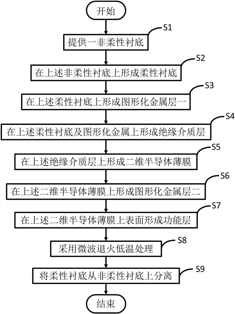
[0056] In order to make the object, technical solution and advantages of the present invention clearer, various embodiments of the present invention will be described in detail below in conjunction with the accompanying drawings. However, those of ordinary skill in the art can understand that, in each implementation manner of the present invention, many technical details are provided for readers to better understand the present application. However, even without these technical details and various changes and modifications based on the following implementation modes, the technical solution claimed in each claim of the present application can be realized.

[0057]The first embodiment of the present invention relates to a method for preparing a two-dimensional flexible ion-sensitive field effect transistor at low temperature. The following combined process figure 1 and gesture Figure 2~8 Be specific. like figure 1 As shown, the specific process includes the following step...


PUM


Abstract

The invention belongs to the technical field of manufacturing of electrochemical sensor devices and particularly discloses a method for low-temperature preparation of a two-dimensional flexible ion-sensitive field effect transistor. The method includes: taking a flexible material as a substrate, depositing a graphic metal layer on the substrate to serve as a back electrode, growing an insulating oxide layer on the back electrode, and transferring a two-dimensional semiconductor film on the insulating medium layer to serve as a conductive channel of a device; forming graphic metal layers on the two-dimensional semiconductor film to serve as source and drain regions of the device; depositing a functional layer material above a channel area. By a microwave annealing process for low-temperature treatment, on the one hand, interface characteristics of layers of the device can be improved so as to eliminate delaying and drifting caused by interface defects; on the other hand, by the aid of the microwave absorption function of the functional layer material and a nano-structure functional layer at an interface of the two-dimensional semiconductor film, applicability to sensing detection in different scenes can be realized. The microwave annealing process has advantages of quickness, low thermal budget, short manufacturing period, low cost and the like.

Description

technical field [0001] The invention relates to the technical field of manufacturing two-dimensional materials and electrochemical sensor devices, in particular to a microwave annealing process. Background technique [0002] In the past few decades, biosensors based on field effect transistors, which convert chemical signals into electrical signal measurements, have the advantages of non-labeling, fast response, low power consumption, portability, low cost, and large-scale integration using microelectronic manufacturing processes. It has been widely researched and applied in the fields of biology, medicine, industrial manufacturing, and environmental detection. The channel materials of field effect transistors usually include three-dimensional bulk silicon, two-dimensional graphene, transition metal sulfides, black phosphorus, one-dimensional nanostructured carbon nanotubes, silicon-based nanowires, etc. Among them, compared with three-dimensional materials, two-dimensional...

Claims


Application Information

Patent Timeline
IPC IPC(8): G01N27/414B82Y40/00
Inventor 曾瑞雪仇志军吴东平
Owner FUDAN UNIV
Why Eureka
Try Eureka