Programmable control micro-fluidic chip based on liquid-liquid electrowetting effect
A microfluidic chip, programming control technology, applied in chemical/physical processes, laboratory containers, chemical/physical/physicochemical processes, etc., can solve the pollution of hydrophobic layer materials, shorten the life of devices, and be easily broken down and other problems, to achieve the effect of good electrowetting, improved service life, and easy removal
- Summary
- Abstract
- Description
- Claims
- Application Information
AI Technical Summary
Problems solved by technology
Method used
Image
Examples
Embodiment 1
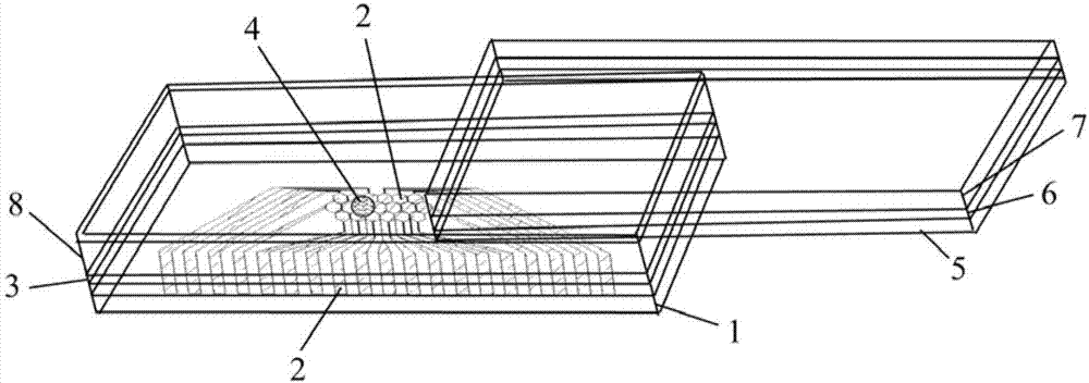
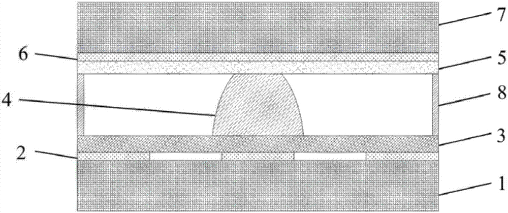
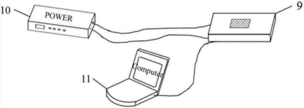
[0034] Such as Figure 1~3 As shown, a programmable control microfluidic chip based on the liquid-liquid electrowetting effect, the microfluidic chip includes from bottom to top: a lower substrate 1, a driving electrode array 2, a hydrophobic insulating layer 3 on the lower substrate , at least one droplet 4, upper substrate hydrophobic layer 5, conductive layer 6, upper substrate 7, cofferdams 8 are added around the upper substrate and the lower substrate to form a closed cavity, the conductive layer 6 is connected to the positive pole of the power supply 10, and the drive The electrode array 2 is connected to the negative electrode of the power supply 10, and the hydrophobic insulating layer 3 of the lower substrate is a solid-liquid composite film structure, which is composed of a porous polymer film and a liquid that can improve the electrowetting performance.
[0035] The electrode array of the lower substrate is connected to the negative pole of the power supply 10, and t...
Embodiment 2
[0050] In this case, glass is preferably used as the upper substrate and the lower substrate, IZO is used as the driving electrode of the lower substrate, and the conductive layer of the upper substrate, perfluorododecyltrichlorosilane is used as the hydrophobic layer of the upper substrate, and the fluorocarbon chain compound FC-43 is filled into the Porous polycarbonate membrane acts as a hydrophobic insulating layer, Figure 6 It is the driving electrode pattern of the embodiment 2, and the half-moon is used as the pattern of the driving electrode, and the number of electrodes can be appropriately added or the electrode arrangement can be adjusted according to different experimental needs.
[0051] The specific process of chip fabrication has been described in detail in Example 1.
Embodiment 3
[0053] In this case, glass is preferably used as the upper substrate and the lower substrate, ZnO is used as the driving electrode of the lower substrate, and the conductive layer of the upper substrate, octadecyltrichlorosilane is used as the hydrophobic layer of the upper substrate, and hexadecane is filled into the porous polyvinylidene fluoride The membrane acts as a hydrophobic insulating layer, Figure 7 It is the driving electrode pattern of embodiment 3, and the hexagon is used as the pattern of the driving electrode, and the number of electrodes can be appropriately added or the arrangement of electrodes can be adjusted according to different experimental needs.
[0054] The specific process of chip fabrication has been described in detail in Example 1.
PUM
 Abstract
Description
Claims
Application Information


