Microfluidic chip based on nanometer drug delivery system screening 3D solid tumor model and preparation method and application thereof
A microfluidic chip and three-dimensional entity technology, which is applied in drug screening, biochemical equipment and methods, compound screening, etc., can solve the problems of accuracy and reliability of analysis results, simple models, and poor integration of drug screening, etc., to achieve easy The effect of mass production, high-throughput detection, and miniaturization
- Summary
- Abstract
- Description
- Claims
- Application Information
AI Technical Summary
Problems solved by technology
Method used
Image
Examples
Embodiment 1
[0074] Embodiment 1 The structure of the chip of the present invention
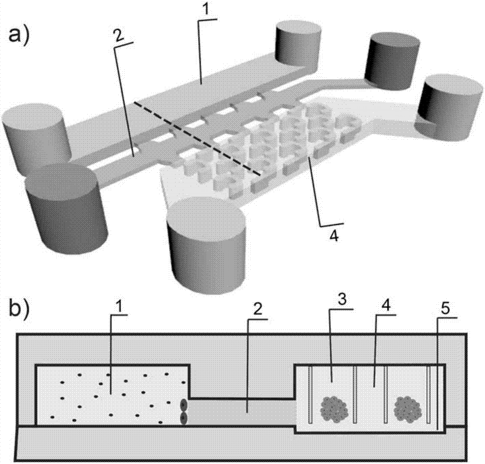
[0075] The chip of the present invention is composed of a bonded PDMS substrate and a cover sheet. Its structure is as figure 1 As shown, the structure of the cover sheet is three parallel channels, and the parallel channels are connected by connecting channels. Among them, including drug perfusion and single-layer blood vessel formation microchannels (1), connecting channels of extracellular matrix (2), and microchannels with 14 "U" groove structures formed by three-dimensional tumor multicellular spheroids (3) ; The substrate has a shallower parallel channel that facilitates cell capture. The microtissue formed by the present invention is very similar to the microenvironment of the solid tumor in the body, and the penetration of the drug in the microtissue can be observed in real time. Its "U" structure corresponds to each well of a 96-well plate, which is conducive to accurate and rapid drug delivery...
Embodiment 2
[0076] Embodiment 2 takes PDMS as the chip of the present invention of substrate and cover sheet to make
[0077] (1) Put the silicon wafer into concentrated H 2 SO 4 / H 2 o 2 (3 / 1) The solution was boiled slightly for 30 minutes, and after cooling, it was taken out and rinsed with deionized water until it became neutral. After ultrasonication of ethanol for 5 minutes, it was heated on a heating plate for 30 minutes.
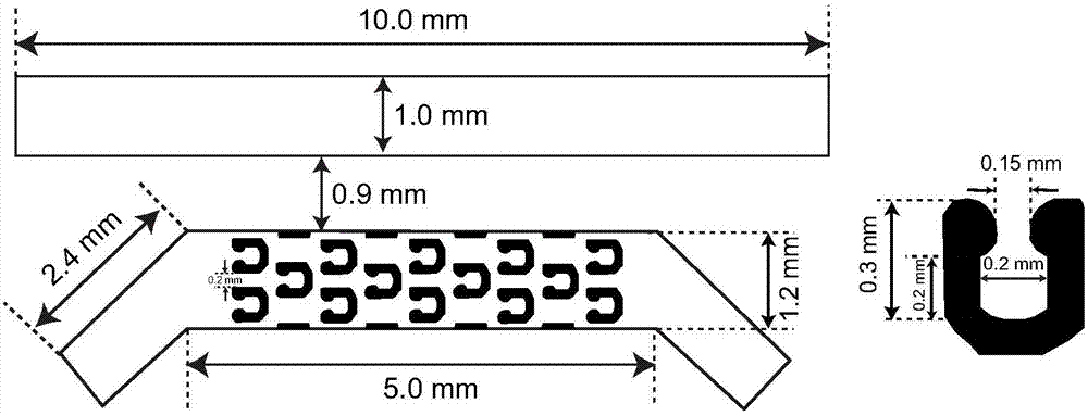
[0078] (2) Spin and coat a thin layer of SU-8 photoresist on the silicon wafer, and make the thickness of the glue layer about 50 μm by controlling the speed of the spin. will have figure 2 The mask of the structure is attached to the silicon wafer, and the ultraviolet light passes through the photomask to expose the photoresist. On the silicon wafer, the thickness of the glue is about 50 μm, which will have image 3 The mask of the structure is bonded to the silicon wafer, and the ultraviolet light is used for secondary exposure, and the unexposed part i...
Embodiment 3
[0081] Example 3 Using the chip prepared in Example 2 to form a three-dimensional solid tumor microtissue
[0082] (1) if figure 1 , the channel (2) of the chip obtained by the present invention is perfused with basement membrane extract (BME) gel to simulate the extracellular matrix, and then the channels (1) and (3) are modified with 1% (w / v) polyvinyl alcohol (PVA) ), to prevent cell adhesion to PDMS.
[0083] (2) Set the concentration to 1×10 5 Tumor cells / mL are poured into the channel (3), so that the cells are uniformly and effectively captured in the "U"-shaped groove, and uniform tumor multicellular microspheres are formed after 48 hours of culture.
[0084] (3) Set the concentration to 5×10 4 Each / mL human umbilical vein endothelial cells (HUVECs) flowed into the channel (1), and the chip was placed vertically to allow the cells to grow on the BME glue. After 2 hours, the chip was placed horizontally to remove excess cells in the channel. Because BME has adhesion f...
PUM
 Abstract
Description
Claims
Application Information


