
An Electrolyte Gate Oxide Semiconductor Phototransistor for Ultraviolet Light Detection

An oxide semiconductor and phototransistor technology, applied in semiconductor devices, circuits, electrical components, etc., can solve problems such as reducing the ultraviolet-visible light rejection ratio, and achieve the goal of increasing the ultraviolet-visible light rejection ratio, reducing the working voltage, and improving the stability. Effect

Active Publication Date: 2019-02-05
SUN YAT SEN UNIV
View PDF4 Cites 0 Cited by
  • Summary
  • Abstract
  • Description
  • Claims
  • Application Information

AI Technical Summary

Problems solved by technology

Moreover, due to the existence of the intermediate state in the oxide, the detector responds to a part of visible light, which greatly reduces the rejection ratio of ultraviolet-visible light.

Method used


Image

  • An Electrolyte Gate Oxide Semiconductor Phototransistor for Ultraviolet Light Detection
  • An Electrolyte Gate Oxide Semiconductor Phototransistor for Ultraviolet Light Detection
  • An Electrolyte Gate Oxide Semiconductor Phototransistor for Ultraviolet Light Detection

Examples


Embodiment 1

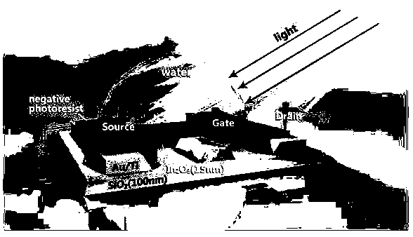
[0030] figure 1 It is a schematic diagram of the structure of the indium oxide thin film transistor ultraviolet light detector in the first embodiment of the present invention, and the substances in the figure have been marked in English.

[0031] The thin film transistor in Embodiment 1 can be manufactured as follows:

[0032] 1) Put the quartz substrate into the MOCVD epitaxial equipment to grow a 15nm indium oxide film. The specific growth conditions are as follows: trimethyl indium is used as the indium source, oxygen is used as the oxygen source, and the epitaxial growth temperature is 421 ° C. The pressure of the reaction chamber is controlled at 7.1 Torr, and the flow rate of trimethylindium is 3×10 -5 mol / min, the flow rate of oxygen is controlled at 7×10 -2 mol / min.

[0033] 2) Then, the grown indium oxide film is masked by photolithography, and the indium oxide is wet-etched to expose the desired shape of the active layer, so that the width-to-length ratio is 2100...


PUM


Abstract

The present invention belongs to the semiconductor optoelectronic device technical field and relates to an electrolyte gate oxide semiconductor phototransistor for ultraviolet light detection. The electrolyte gate oxide semiconductor phototransistor for the ultraviolet light detection includes a polycrystalline or single-crystal semiconductor active layer which is located on an insulating substrate, a source / drain electrode, an insulating protective layer, an electrolyte gate dielectric which covers the active layer and the protective layer, and a gate electrode which contacts with the electrolyte. The electrolyte gate oxide semiconductor phototransistor is provided with an oxide semiconductor material having a wide optical bandgap, so that the electrolyte gate oxide semiconductor phototransistor can be low in cost and is transparent; the cut-off wavelength of the detector can be achieved by adjusting the compositions of the oxide semiconductor material; the oxide semiconductor ultraviolet detector is based on a field effect transistor structure, so that the oxide semiconductor ultraviolet detector has higher responsiveness, a higher signal to noise ratio and higher stability, and has no requirements for harsh vacuum environments; and the electrolyte having a high dielectric constant is adopted as the gate dielectric layer, and therefore, the structure of the phototransistor is simple, and at the same time, the working voltage of the phototransistor is greatly reduced.

Description

technical field [0001] The present invention relates to the technical field of semiconductor optoelectronic devices, and more specifically relates to an electrolyte gate oxide semiconductor phototransistor for ultraviolet light detection. Background technique [0002] Ultraviolet (UV) detection technology is a photoelectric detection technology with high application value in military and civilian applications, and is widely used in sky communication, ozone detection, pollutant detection, flame detection and other fields. [0003] Ultraviolet detectors can generally be divided into three different structures: photoresistors, photodiodes, and phototransistors. Among them, phototransistors have attracted widespread attention in the industry due to their high responsivity and high signal-to-noise ratio (CN201110206933.2, etc.). In addition, as a three-terminal device, the phototransistor has the functions of switching, driving, and reading, and can be used in the active array of...

Claims


Application Information

Patent Timeline
Patent Type & Authority Patents(China)
IPC IPC(8): H01L31/113H01L31/0296
CPCH01L31/0296H01L31/1136
Inventor 蔡广烁王钢裴艳丽
Owner SUN YAT SEN UNIV
Learn More