A kind of bidirectional light emitting diode and its preparation method

A technology of light-emitting diodes and diodes, applied in semiconductor devices, electrical components, circuits, etc., can solve the problems of increasing electron recombination rate, increasing luminescence, and failing to solve the problem of device heating, so as to increase electron injection efficiency, improve stability, and improve The effect of thermal conductivity

Active Publication Date: 2020-03-31
SOUTHEAST UNIV
View PDF7 Cites 0 Cited by
  • Summary
  • Abstract
  • Description
  • Claims
  • Application Information

AI Technical Summary

Problems solved by technology

Although this method can effectively increase the recombination rate of electrons to increase luminescence, it still cannot solve the problem of heat generation of the device.

Method used


Image

  • A kind of bidirectional light emitting diode and its preparation method
  • A kind of bidirectional light emitting diode and its preparation method
  • A kind of bidirectional light emitting diode and its preparation method

Examples


Embodiment 1

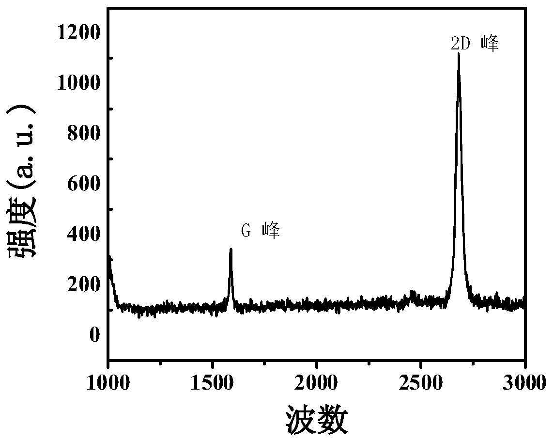
[0037] The first step: ZnO powder and carbon powder with a purity of 99.99wt% are mixed and ground according to the mass ratio of 1:1, and the mixture is filled into a ceramic boat; a silicon wafer with a size close to the opening area of ​​the ceramic boat is taken, and the acetone , anhydrous ethanol and deionized water, followed by ultrasonic cleaning and nitrogen flushing, the silicon wafer was covered with the polished side down and above the ceramic boat; then the ceramic boat was pushed into a tube furnace with a temperature of 1050 ° C; after 60 minutes of reaction , to form larger ZnO microrod arrays grown on the surface of the silicon wafer;

[0038] The second step: using 50g / L FeCl 3 Solution processing copper-based graphene, the specific method is to cut the PMMA spin-coated copper-based graphene into 0.5*0.5mm squares, and then place it on FeCl 3 Soak in the solution for 1 hour, then use a glass slide to resuspend the FeCl 3 The graphene in the solution was tra...

Embodiment 2

[0044] The first step: ZnO powder and carbon powder with a purity of 99wt% are mixed and ground according to a mass ratio of 1:3, and the mixture is filled into a ceramic boat; After ultrasonic cleaning with water ethanol and deionized water in sequence, after drying with nitrogen gas, place the polished side of the silicon wafer down and cover the top of the ceramic boat; then push the ceramic boat into a tube furnace with a temperature of 1050°C; after 80 minutes of reaction , to form larger ZnO microrod arrays grown on the surface of the silicon wafer;

[0045] The second step: using 20g / L FeCl 3 Solution processing copper-based graphene, the specific method is to cut the PMMA spin-coated copper-based graphene into 0.5*0.5mm squares, and then place it on FeCl 3 Soak in the solution for 2 hours, then use a glass slide to resuspend the FeCl 3 Transfer the graphene in the solution to clean water and clean it, then transfer it to a p-GaN substrate, then dry it in a drying ove...

Embodiment 3

[0051] The first step: ZnO powder and carbon powder with a purity of 99wt% are mixed and ground according to a mass ratio of 1:3, and the mixture is filled into a ceramic boat; After ultrasonic cleaning with water ethanol and deionized water in sequence, after drying with nitrogen gas, place the polished side of the silicon wafer down and cover the top of the ceramic boat; then push the ceramic boat into a tube furnace at a temperature of 950 °C; after 150 minutes of reaction , to form larger ZnO microrod arrays grown on the surface of the silicon wafer;

[0052] The second step: using 40g / L FeCl 3 Solution processing copper-based graphene, the specific method is to cut the PMMA spin-coated copper-based graphene into 0.5*0.5mm squares, and then place it on FeCl 3 Soak in the solution for 1.5 hours, then slide the suspension in FeCl 3 The graphene in the solution was transferred to clean water and cleaned, then transferred to the p-GaN layer, and then dried in a drying oven a...


PUM

PropertyMeasurementUnit
thicknessaaaaaaaaaa
lengthaaaaaaaaaa
diameteraaaaaaaaaa

Abstract

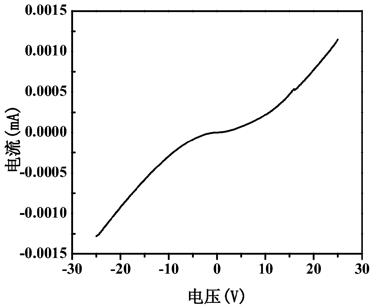
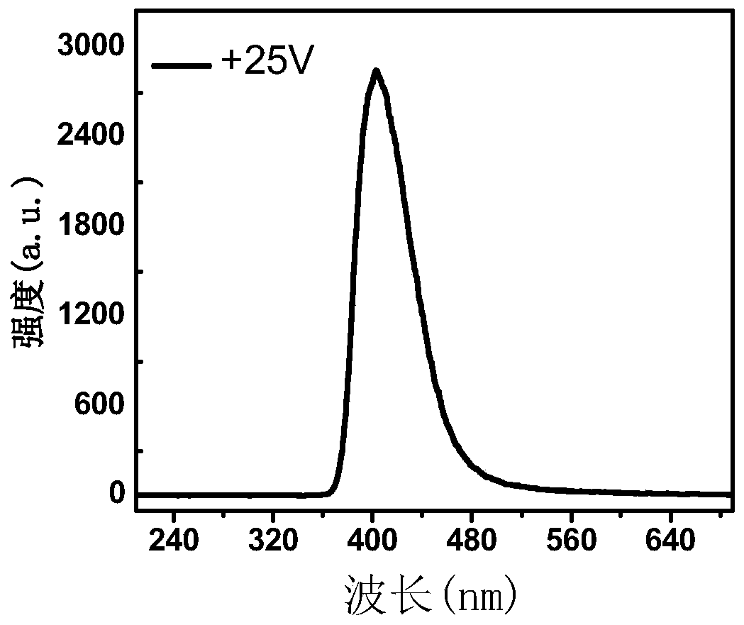
The invention discloses a bidirectional light emitting diode and a manufacturing method thereof. The diode is a GaN-graphene-MgO-ZnO micro-rod bidirectional light emitting diode and sequentially comprises a p-type GaN layer, a graphene layer, a MaO layer and a ZnO micro-rod from down to up, a side electrode is arranged on the gallium nitride layer, and a right side electrode is arranged on the zinc oxide layer. The method comprises steps that the graphene layer is added on the GaN layer; 2), the MgO layer is plated on an upper surface of the graphene layer; 3), a ZnO micro-rod array is manufactured on a silicon chip to form a GaN-graphene-MgO-ZnO heterojunction; and 5), the side electrode is arranged on the surface of the GaN layer, and the right side electrode covers the zinc micro-rod surface. The bidirectional light emitting diode is advantaged in that current injection of a graphene enhancement junction is utilized, luminescence can be realized under positive and negative biases, high brightness is realized, the manufacturing process is simple, and cost is low.

Description

technical field [0001] The invention relates to a bidirectional light emitting diode and a preparation method thereof, belonging to the field of light emitting diodes. Background technique [0002] As a semiconductor material with direct band gap and wide bandgap, zinc oxide (ZnO) has an exciton binding energy up to 60meV, which is much higher than that of gallium nitride (GaN) and thermal ionization energy. Therefore, the exciton It can exist stably at room temperature; compared with other semiconductor materials, ZnO is an ultraviolet optoelectronic semiconductor material that is more suitable for use at room temperature or higher; since Japanese scientists and American scientists have successively discovered ZnO thin films and nanowires Since the ultraviolet radiation, ZnO has become an ideal material for designing ultraviolet light-emitting devices. However, due to the self-doping characteristics, it is difficult to obtain stable p-doped ZnO. In order to construct heter...

Claims


Application Information

Patent Timeline
Patent Type & Authority Patents(China)
IPC IPC(8): H01L33/00H01L33/26
Inventor 徐春祥秦飞飞石增良游道通徐巍
Owner SOUTHEAST UNIV
Why Eureka
Try Eureka