Vertical Interconnect Structure of W-Band Gallium Arsenide Monolithic Integrated Circuit 3D System-in-Package

A monolithic integrated circuit, system-in-package technology, applied in the field of electromagnetic fields and microwaves, can solve problems such as bulky volume and weight, performance limitations, unsuitable for mass production, etc., to achieve the effect of enriching performance and reducing costs

Active Publication Date: 2020-06-05
NO 55 INST CHINA ELECTRONIC SCI & TECHNOLOGYGROUP CO LTD
View PDF6 Cites 0 Cited by
  • Summary
  • Abstract
  • Description
  • Claims
  • Application Information

AI Technical Summary

Problems solved by technology

[0003] For precision guidance of missile weapon systems, security imaging in the security field, and ultra-wideband intersatellite communication, the millimeter-wave front-end system working in the W-band (94GHz) is favored by researchers from all over the world. The development in this area is mainly reflected in The following three aspects: (1) The millimeter-wave front-end represented by the system on chip, that is, the entire front-end system is directly integrated on the semiconductor wafer. This method is only applicable to specific application backgrounds due to cost and development time cycle factors, and the on-chip A semiconductor manufacturing process, the performance of each component is often subject to certain restrictions, and the radiation efficiency of the on-chip antenna is also one of its development constraints; (2) The W-band front-end module assembly of the traditional waveguide cavity is limited by the machining accuracy The restriction is not suitable for mass production, and requires the special gold wire bonding operation of mature craftsmen, the batch consistency of the product is not well guaranteed, and the bulky volume and weight are also one of its defects; (3) Combining System-in-package of semiconductor and substrate processing technology, that is, to organically integrate existing chip modules through various substrates and interconnections to form a packaged module with certain performance
[0004] In the W-band system-in-package, the flip-chip process is one of the key interconnection processes. However, at present, in addition to the silicon-germanium (SiGe) chip that can be flip-chip onto the substrate, the GaAs chip of the traditional microstrip line process still needs There are also a few GaAs chips using coplanar waveguide and input-output backhole technology that are suitable for flip-chip technology through gold wire bonding to the substrate substrate. However, GaAs chips with corresponding functions need to be specially developed, and the cost is relatively high, and the performance is also limited. , not suitable for the current W-band system-in-package application development
On the other hand, W-band system-in-package currently integrates antennas and transceiver channels basically in a two-dimensional way. Although the concept of vertical three-dimensional system-in-package has been proposed, the lack of vertical interconnection structure limits the use of GaAs chips in this area. Application and Development of Quasi-3D System-in-Package

Method used


Image

  • Vertical Interconnect Structure of W-Band Gallium Arsenide Monolithic Integrated Circuit 3D System-in-Package
  • Vertical Interconnect Structure of W-Band Gallium Arsenide Monolithic Integrated Circuit 3D System-in-Package
  • Vertical Interconnect Structure of W-Band Gallium Arsenide Monolithic Integrated Circuit 3D System-in-Package

Examples


Embodiment

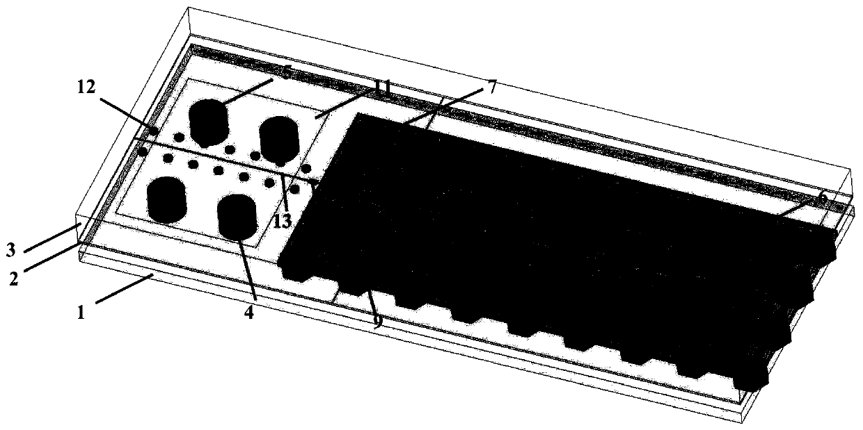
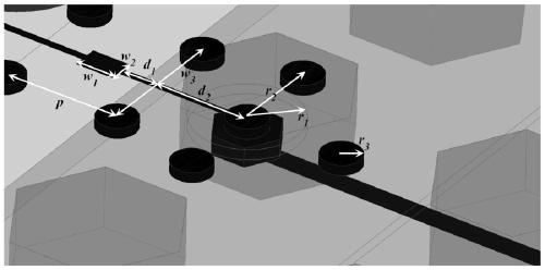
[0022] A new W-band GaAs chip three-dimensional integrated system-in-package vertical interconnection structure, such as figure 1 As shown, it includes a substrate dielectric substrate 1, a BCB dielectric 2 on a silicon substrate, a silicon substrate 3, a metallization column 4 in the substrate dielectric substrate, a first solder ball 5 interconnected between the BCB surface metal and the substrate dielectric substrate surface metal, Substrate dielectric pillar array 6 in the substrate, GaAs chip substrate 7, 50 ohm microstrip line 8 on the GaAs chip, metal plane 9 on the upper and lower surfaces of the BCB medium, circular grooves 10 on the metal plane on the upper and lower surfaces of the BCB medium, the substrate The metal 11 on the upper surface of the dielectric substrate, the metallization column 12 in the BCB medium, the central conductor 13 of the 50-ohm planar coaxial transmission line in the BCB medium, the capacitance compensation sheet 14 on the center conductor o...


PUM

PropertyMeasurementUnit
thicknessaaaaaaaaaa

Abstract

The invention discloses a W-band gallium arsenide monolithic integrated circuit three-dimensional system-level package vertical interconnection structure, the vertical interconnection structure includes GaAs monolithic integrated circuit itself 50 ohm microstrip transmission line, silicon substrate via hole and flip chip A quasi-coaxial structure composed of solder balls, a 50-ohm planar coaxial transmission line structure with capacitance compensation on a silicon substrate; a GaAs monolithic integrated circuit is installed on the substrate dielectric substrate, and flipped on the upper silicon substrate; on the silicon substrate The 50-ohm planar coaxial-like transmission line structure has an impedance matching structure. The present invention can realize the broadband transmission of millimeter-wave signals in GaAs monolithic integrated circuits in antenna-feeder integrated three-dimensional vertical interconnection system-level packaging architecture, and through the vertical interconnection structure, GaAs monolithic integrated circuits can be effectively integrated into miniaturized In the antenna-feeder integrated 3D microsystem, the types and performances of the W-band system and package optional chips are greatly enriched.

Description

technical field [0001] The invention belongs to the technical field of electromagnetic fields and microwaves, and in particular relates to a vertical interconnection structure of a three-dimensional system-level package of a W-band gallium arsenide monolithic integrated circuit. Background technique [0002] With the continuous advancement of semiconductor process technology, military and civilian wireless front-end systems are also developing in the direction of high frequency. At present, monolithic integrated circuits based on processes such as gallium arsenide (GaAs), gallium nitride (GaN) and indium phosphide (InP) have operating frequencies as high as 1 THz; the operating frequency of millimeter-wave module components is also extending towards the THz frequency band. [0003] For precision guidance of missile weapon systems, security imaging in the security field, and ultra-wideband intersatellite communication, the millimeter-wave front-end system working in the W-ban...

Claims


Application Information

Patent Timeline
Patent Type & Authority Patents(China)
IPC IPC(8): H01L25/00H01L23/66H01L23/538H01L23/498
CPCH01L23/49827H01L23/5384H01L23/66H01L25/00H01L2223/6627
Inventor 施永荣张君直
Owner NO 55 INST CHINA ELECTRONIC SCI & TECHNOLOGYGROUP CO LTD
Why Eureka
Try Eureka