

A titanium nitride atomic layer deposition device and its deposition method
A technology of atomic layer deposition and titanium nitride, which is applied in the direction of coating, gaseous chemical plating, metal material coating process, etc., can solve the problems of polluting the substrate surface, not being effective, and having no heating function, so as to avoid gas Effects of handling system settings, reducing undesired reactions, and reducing particle generation
- Summary
- Abstract
- Description
- Claims
- Application Information
AI Technical Summary
Problems solved by technology
Method used
Image

Examples
Embodiment Construction
[0064] The specific embodiment of the present invention will be further described in detail below in conjunction with the accompanying drawings.
[0065] It should be noted that, in the following specific embodiments, when describing the embodiments of the present invention in detail, in order to clearly show the structure of the present invention for the convenience of description, the structures in the drawings are not drawn according to the general scale, and are drawn Partial magnification, deformation and simplification are included, therefore, it should be avoided to be interpreted as a limitation of the present invention.
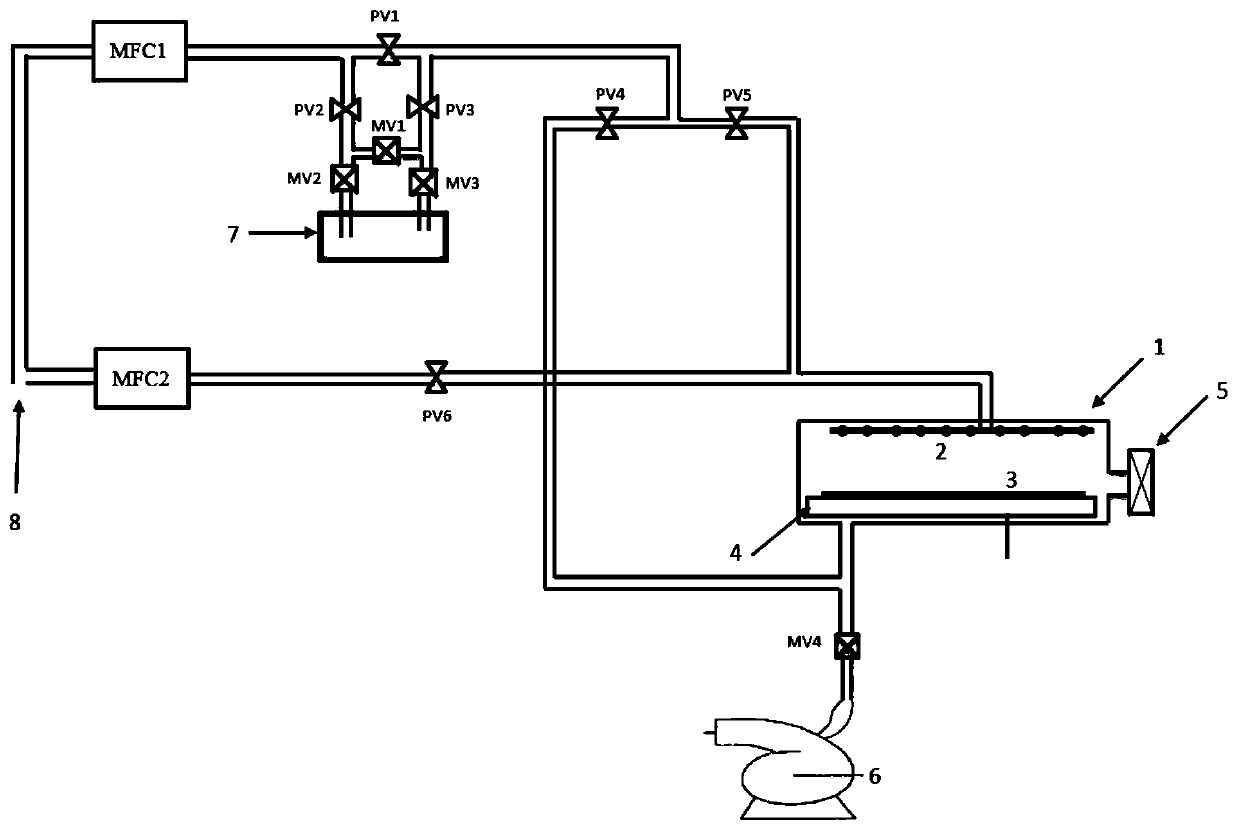
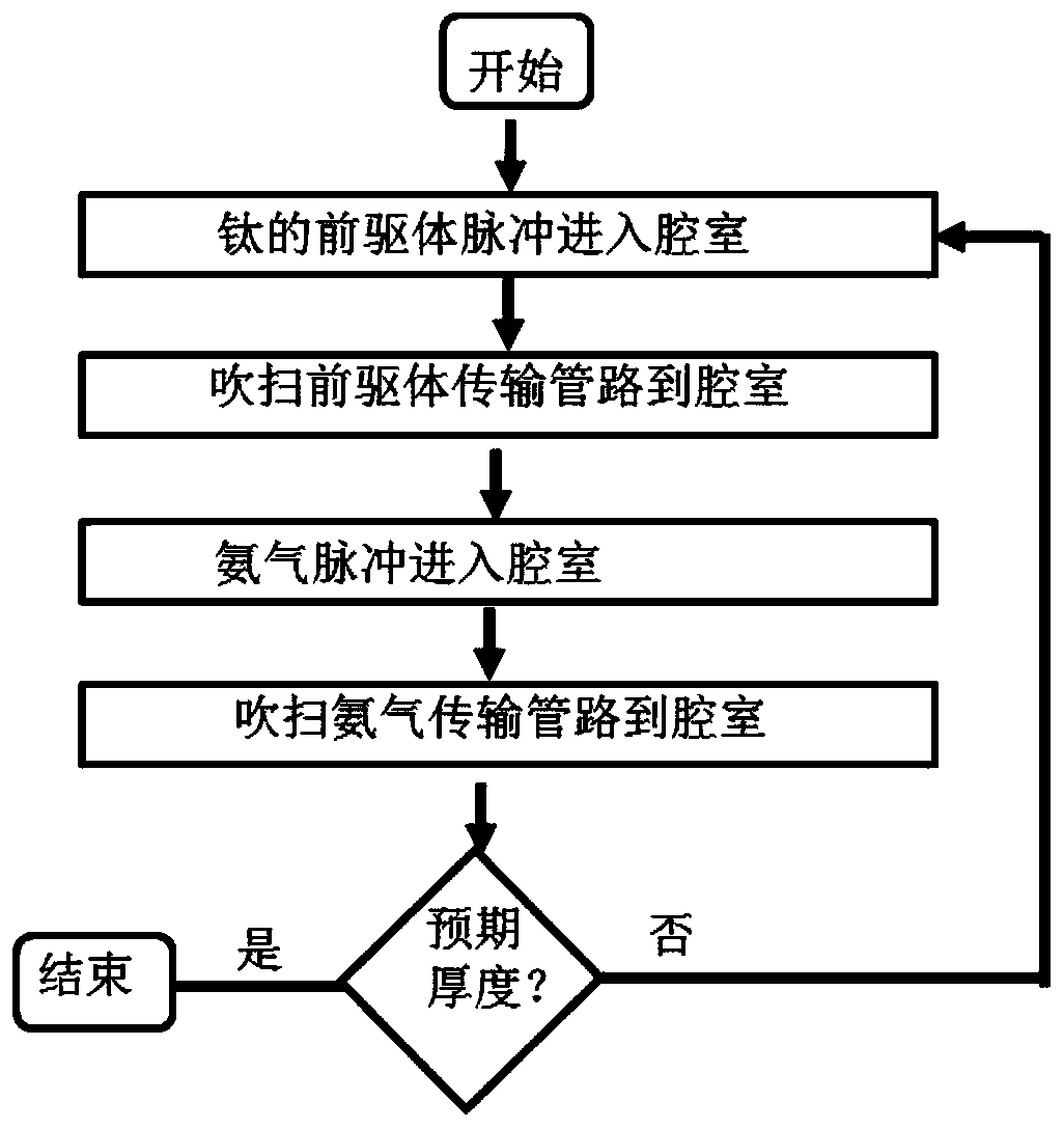
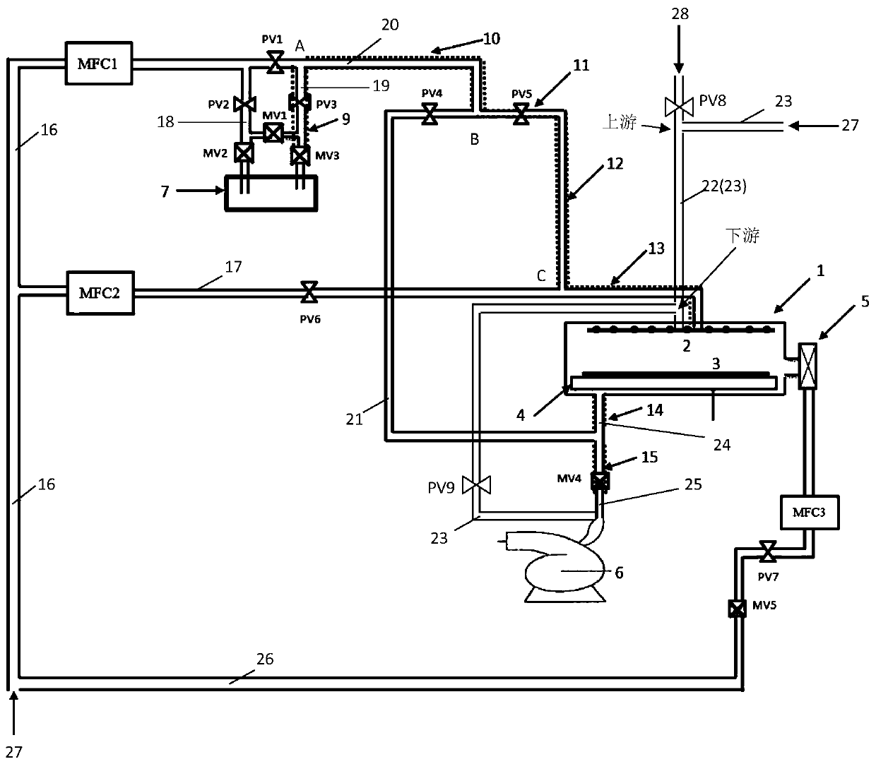
[0066] In the following specific embodiments of the present invention, please refer to image 3 , image 3 It is a schematic structural diagram of a titanium nitride atomic layer deposition device according to a preferred embodiment of the present invention. Such as image 3 As shown, a titanium nitride atomic layer deposition device of the presen...
PUM
 Abstract
Description
Claims
Application Information