Method for fabricating thin film circuits on warped co-fired ceramic substrate

A technology of thin-film circuits and co-fired ceramics, which is used in the manufacture of circuits, electrical components, semiconductor/solid-state devices, etc., can solve the uneven thickness of the dielectric layer and weaken the adhesion at the interface between the co-fired ceramic substrate and the organic dielectric layer of the thin-film circuit. , Substrate scrap, etc.

Active Publication Date: 2018-04-03
苏州华博电子科技有限公司
View PDF4 Cites 3 Cited by
  • Summary
  • Abstract
  • Description
  • Claims
  • Application Information

AI Technical Summary

Problems solved by technology

[0004] However, polishing the warped co-fired ceramic substrate will make the thickness of the dielectric layer on the surface of the substrate uneven, which will affect the high-frequency electrical performance, and even expose the internal metal wires, making the entire substrate scrapped; for co-fired ceramics Although the polishing of the substrate meets the needs of making precision thin film circuits,

Method used


Image

  • Method for fabricating thin film circuits on warped co-fired ceramic substrate
  • Method for fabricating thin film circuits on warped co-fired ceramic substrate

Examples


Embodiment Construction

[0027] Specific embodiments of the present invention will be described in detail below in conjunction with the accompanying drawings.

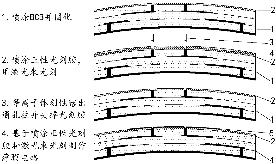
[0028] Such as figure 2 As shown, a method for manufacturing a thin film circuit on a warped co-fired ceramic substrate comprises the following steps:

[0029] 1) The co-fired ceramic substrate is selected as a 10-layer LTCC instant-fired substrate. After the sintering furnace is taken out, it is stored in a clean box to avoid contamination. The warpage is 30 μm and the surface roughness is 250 nm; bake at 120 ° C for two hours before use. Spray BCB and cure: first spray BCB adhesion enhancer AP3000 with a molecular layer thickness, blow dry with nitrogen, then spray BCB3022-35 glue, and then cure in a nitrogen atmosphere furnace according to the BCB curing temperature curve, and the thickness after curing is 1 μm;

[0030] 2) Spray positive photoresist AZ4620 on the cured BCB dielectric layer, and use the laser beam of 355nm laser drilling ...


PUM


Abstract

The invention discloses a method for fabricating thin film circuits on a warped co-fired ceramic substrate in a polishing-free manner. The method comprises the following steps of 1), spraying the warped co-fired ceramic substrate with a BCB glue solution, and then performing solidification in a nitrogen atmosphere furnace according to a BCB solidification temperature curve; 2), spraying a solidified BCB medium layer with positive photoresist, exposing the positive photoresist over against a through hole column by using laser beams after pre-baking, performing development to remove the exposedpositive photoresist over against the through hole column, and performing post-baking on the photoresist; 3), etching a BCB medium by using oxygen/carbon tetrafluoride plasmas to expose the through hole column, and then removing a residual photoresist mask by using the oxygen plasmas or a photoresist removal solution; 4), based on the positive photoresist spraying and the laser beam photoetching,making a thin film circuit of a bottom layer; and 5), based on the positive photoresist spraying and the laser beam photoetching, making thin film circuits of subsequent layers.

Description

technical field [0001] The invention relates to a manufacturing method of a thin film circuit on a warped co-fired ceramic substrate. Background technique [0002] Co-fired ceramic substrate is a kind of multi-chip module (Milti-chip-module, MCM) packaging substrate developed to adapt to the high integration and miniaturization of electronic systems, that is, MCM-C packaging substrate, including low-temperature co-fired ceramics (LTCC) substrates and high temperature co-fired ceramic substrates (HTCC). Co-fired ceramic substrates have high integration and good heat dissipation performance, but the circuit accuracy, circuit density, signal delay, and high-frequency performance are not as good as thin-film circuits. Therefore, in order to improve the performance of the entire packaging substrate, thin-film circuits are fabricated on the co-fired ceramic substrate to form a co-fired ceramic-thin film hybrid packaging substrate, that is, the MCM-C / D packaging substrate. [000...

Claims


Application Information

Patent Timeline
IPC IPC(8): H01L21/70H01L21/027
CPCH01L21/0275H01L21/707
Inventor 王列松薛新忠高永全朱小明陈洋
Owner 苏州华博电子科技有限公司
Why Eureka
Try Eureka