Epitaxial growth method of high-resistance GaN thin film

A technology of epitaxial growth and thin film, which is applied in the direction of electrical components, semiconductor/solid-state device manufacturing, circuits, etc., can solve problems such as the decrease of two-dimensional electron gas mobility, affect device performance, and restrict device performance, so as to reduce Ga gap and crystal The effect of high quality and improved surface flatness

Active Publication Date: 2018-04-06
NO 55 INST CHINA ELECTRONIC SCI & TECHNOLOGYGROUP CO LTD
View PDF5 Cites 4 Cited by
  • Summary
  • Abstract
  • Description
  • Claims
  • Application Information

AI Technical Summary

Problems solved by technology

Compared with these methods, the method of unintentional doping does not require additional doping sources, and can avoid the influence of dopant sources polluting the reaction chamber and memory effects, but this method usually sacrifices the quality of material crystals, and introduces A large number of edge dislocations lead to a decrease in the mobility of the two-dimensional electron gas, which restricts the further improvement of device performance; the p-type doping compensation method requires a specific doping source, and the advantage of this method is that it has good repeatability, but The memory effect of the dopant source will lead to system contamination, resulting in impurity scattering benefits affecting device performance

Method used


Image

  • Epitaxial growth method of high-resistance GaN thin film

Examples


Embodiment 1

[0022] 1) Choose a slice c Surface sapphire substrate, transfer it to the reaction chamber of MOCVD equipment, in H 2 The temperature was raised to 1100°C under the atmosphere, and the substrate was baked for 5 minutes to clean the surface of the substrate;

[0023] 2) Lower the temperature to 550°C, and feed TMGa and NH into the reaction chamber at the same time 3 ,TMGa / NH 3 The molar ratio (Ⅴ / Ⅲ ratio) is 1500, H 2 As the carrier gas, the pressure of the reaction chamber is 500torr, and the nucleation layer is grown, and the thickness of the nucleation layer is 25nm;

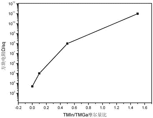
[0024] 3) in NH 3 Under protection, the temperature was increased to 1050 °C, and TMGa and TMIn were introduced into the reaction chamber at the same time to carry out epitaxial growth of high-resistance GaN thin films. The molar ratio of TMIn / TMGa was 0.5, the V / III ratio was 1000, and the H 2 It is the carrier gas, the reaction chamber pressure is 300torr, and the film thickness is 2μm;

[0025] 4) Cool...

Embodiment 2

[0027] 1) Select a Si-faced 4H-SiC substrate, transfer it to the reaction chamber of the MOCVD equipment, and 2 Raise the temperature to 1200°C under the atmosphere, bake the substrate for 5 minutes, and clean the surface of the substrate;

[0028] 2) Lower the temperature to 900°C and feed TMAl and NH into the reaction chamber at the same time 3 , V / III ratio is 1000, H 2 As the carrier gas, the pressure of the reaction chamber is 100torr, and the nucleation layer is grown, and the thickness of the nucleation layer is 60nm;

[0029] 3) in NH 3 Under protection, the temperature was increased to 1100 ° C, and TMGa and TMIn were introduced into the reaction chamber at the same time to carry out epitaxial growth of high-resistance GaN thin films. The molar ratio of TMIn / TMGa was 1.5, and the V / III ratio was 2500. N 2 It is the carrier gas, the reaction chamber pressure is 300torr, and the film thickness is 2μm;

[0030] 4) Cool down to room temperature, and transfer the GaN t...

Embodiment 3

[0032] 1) Select a (111) Si substrate, transfer it to the reaction chamber of the MOCVD equipment, in the H 2 The temperature was raised to 1050°C under the atmosphere, and the substrate was baked for 5 minutes to clean the surface of the substrate;

[0033] 2) Lower the temperature to 850°C, and feed TMAl and NH into the reaction chamber at the same time 3 , V / III ratio is 1000, H 2 As the carrier gas, the pressure of the reaction chamber is 100torr, and the nucleation layer is grown, and the thickness of the nucleation layer is 30nm;

[0034]3) in NH 3 Under protection, raise the temperature to 1020°C, and at the same time feed TMGa and TMIn into the reaction chamber to carry out epitaxial growth of high-resistance GaN thin films. 2 The mixed gas is the carrier gas, the reaction chamber pressure is 100torr, and the film thickness is 4μm;

[0035] 4) Cool down to room temperature, and transfer the GaN thin film material out of the MOCVD equipment.


PUM


Abstract

The invention relates to an epitaxial growth method of a high-resistance GaN thin film. The method is performed in MOCVD equipment and includes a substrate baking stage, a nucleation stage and an epitaxial growth stage. The method is characterized in that a metal organic matter trimethylindium is used as a C impurity doping source during the epitaxial growth stage. With the method adopted, the high resistance of the GaN thin film can be achieved; the TMIn is unlikely to form In-N bonds in crystal lattices under high temperature, and therefore, high growth temperature can assist in avoiding theformation of InGaN alloys and ensuring the integrity of the lattice structure of the GaN thin film; the concentration of C impurities in a GaN epitaxial layer can be effectively controlled by changing the flow rate of the dopant TMIn, and therefore, doping efficiency is high, and repeatability is stable; and a doping source pipeline is not required to be added into an MOCVD system, other C dopingsources are not required to be installed, and therefore, the resources of existing device can be fully utilized. The method is of simplicity and easy to operate. The epitaxial material has good performance. The high-quality and low-cost growth of the high-resistance GaN thin film can be realized.

Description

technical field [0001] The invention relates to a method for epitaxial growth of a high-resistance GaN thin film, which belongs to the technical field of semiconductors. Background technique [0002] As the third-generation wide-bandgap semiconductor material, GaN not only has a wide bandgap (3.4eV), but also has the characteristics of large thermal conductivity, high electron saturation rate, strong breakdown field and good thermal stability. High-frequency, high-voltage and high-power devices have attracted much attention. HEMT devices based on AlGaN / GaN heterojunction have excellent characteristics such as large breakdown voltage, high saturation electron velocity, and high 2DEG concentration. However, there are still many key technologies that need further research. Among them, the high-resistance GaN buffer layer is an important factor affecting the leakage problem of AlGaN / GaN HEMTs devices. For microwave power devices, the leakage of the buffer layer will directly ...

Claims


Application Information

Patent Timeline
Patent Type & Authority Applications(China)
IPC IPC(8): H01L21/02
CPCH01L21/0254H01L21/02579H01L21/0262
Inventor 罗伟科杨乾坤李忠辉
Owner NO 55 INST CHINA ELECTRONIC SCI & TECHNOLOGYGROUP CO LTD
Why Eureka
Try Eureka