

Controllable quantum dot array preparing method based on photo-thermal effect
A technology of photothermal effect and quantum dots, which is applied in nanotechnology for materials and surface science, semiconductor/solid-state device manufacturing, electrical components, etc., can solve the problem of not being able to balance cost and effect, and achieve low cost and broad application prospects , The effect of simple process
- Summary
- Abstract
- Description
- Claims
- Application Information
AI Technical Summary
Problems solved by technology
Method used
Image

Examples
Embodiment 1
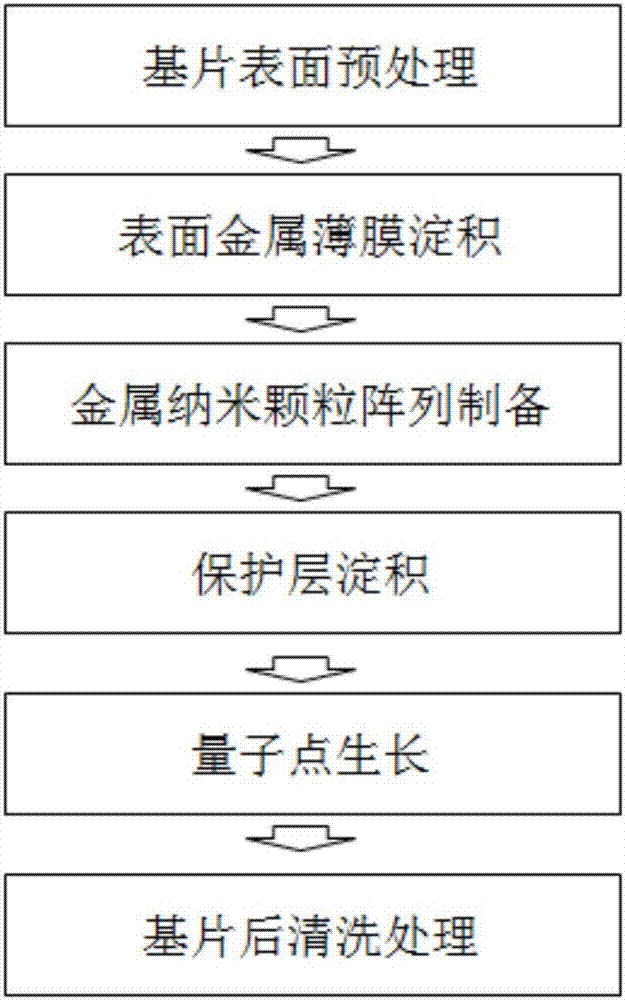
[0022] Step 1, immerse the quartz glass substrate in acetone for 15 minutes for ultrasonic cleaning, ethanol for 10 minutes for ultrasonic cleaning to remove surface impurities, and then take it out. After rinsing with deionized water for 45 seconds, dry the residual moisture with nitrogen gas. Put the treated substrate into the plasma cleaning machine, vacuum to 10 -1 Pa, feed oxygen to 10Pa, wash for 5 minutes and take it out.
[0023] Step 2, placing the cleaned substrate on the sample stage of the ion sputtering device, and then placing the Au metal target on the target stage. Close the sputtering chamber cover and pump the vacuum to about 10Pa, set the ionization current to 3mA, and apply a voltage to the electrode of the ion sputtering device. Deposited on a quartz glass substrate at a high speed. The Au deposition time was controlled to be 50s to obtain a 10nm thick Au film.
[0024] Step 3, move the substrate deposited with the Au film into the annealing furnace, ...
Embodiment 2
[0029] Step 1: Dip the GaN(0001) substrate into acetone and ultrasonically clean it for 15 minutes, and then ultrasonically clean it with ethanol for 10 minutes to remove surface impurities and take it out. After rinsing with deionized water for 45 seconds, dry the residual moisture with nitrogen gas. Put the treated substrate into the plasma cleaning machine, vacuum to 10 -1 Pa, feed oxygen to 10Pa, wash for 5 minutes and take it out.
[0030] Step 2: Place the cleaned substrate on the sample stage of the ion sputtering device, and then place the Ag metal target on the target stage (cathode). Close the sputtering chamber cover and pump the vacuum to about 10Pa, set the ionization current to 3mA, and apply a voltage to the electrode of the ion sputtering device. The speed is deposited on the GaN (0001) substrate. The Ag deposition time was controlled to be 20s to obtain a 5nm thick Ag film. The target material is replaced with metal Pt, and the deposition operation is rep...
Embodiment 3
[0036] Step 1: immerse the Si substrate in acetone for 15 minutes and ultrasonically clean it with ethanol for 10 minutes to remove surface impurities and then take it out. After rinsing with deionized water for 45 seconds, dry the residual moisture with nitrogen gas. Put the processed substrate into the plasma cleaning machine, vacuum to 10 -1 Pa, feed oxygen to 10Pa, wash for 5 minutes and take it out.
[0037] Step 2: Place the cleaned substrate on the sample stage of the ion sputtering device, and then place the Al metal target on the target stage. Close the sputter chamber lid and pull the vacuum to about 10 -4 Pa, enter Ar gas to 10Pa, set the ionization current to 4mA, and apply a voltage on the electrode of the ion sputtering device, after the current is stable, make Al deposited on the substrate at a high speed. The Al deposition time is controlled to be 100s to obtain a 20nm thick Al film.
[0038] Step 3: using a photolithography method to etch the Al thin fil...
PUM
| Property | Measurement | Unit |
|---|---|---|
| Thickness | aaaaa | aaaaa |
| Thickness | aaaaa | aaaaa |
| Diameter | aaaaa | aaaaa |
Abstract
Description
Claims
Application Information