Device and method for preparing non-polar indium nitride nanocrystalline thin film

An indium nitride nanometer and a technology for preparing devices, which are applied in chemical instruments and methods, single crystal growth, crystal growth, etc., can solve the problems of unsuitability for commercial development, poor quality of InN films, unfavorable thermal stability, etc. The effect of poor thermal stability, uniform morphology and size, and high crystal quality

Active Publication Date: 2018-05-22
SHENYANG LIGONG UNIV
View PDF4 Cites 3 Cited by
  • Summary
  • Abstract
  • Description
  • Claims
  • Application Information

AI Technical Summary

Problems solved by technology

The reactants used in the MOCVD preparation method are organic sources, and anti-virus measures need to be taken, and the MOCVD method requires a higher temperature (about 750-1000 ° C), which is not conducive to the thermal stability of InN
The PA-MBE method has a high degree of vacuum, the reaction source used is simple, and can achieve high-quality InN film epitaxial growth, but due to its own characteristics, the PA-MBE method requires about 300W of high-frequency radio frequency power, and it is expensive. Not suitable for commercial development
InN films prepared by magnetron sputtering have poor quality, poor crystallization, and uneven growth

Method used


Image

  • Device and method for preparing non-polar indium nitride nanocrystalline thin film
  • Device and method for preparing non-polar indium nitride nanocrystalline thin film
  • Device and method for preparing non-polar indium nitride nanocrystalline thin film

Examples


Embodiment 1

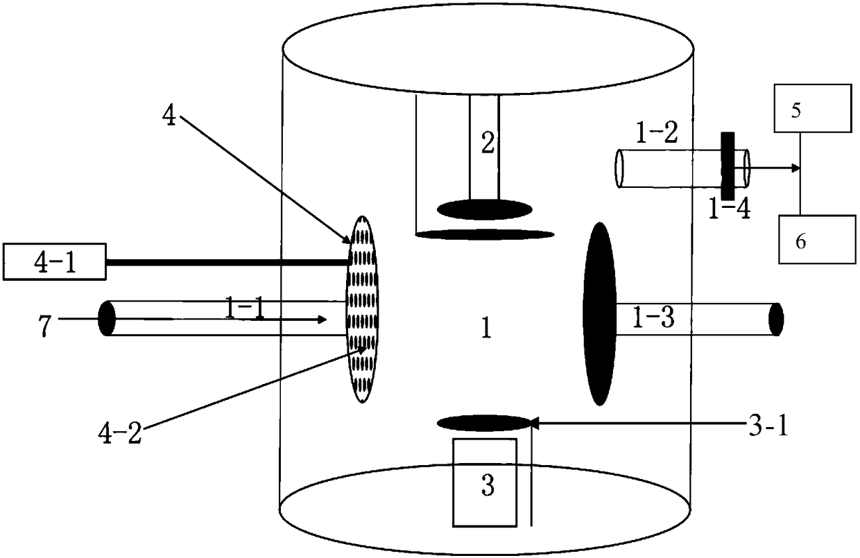
[0055] A device for preparing a non-polar indium nitride nanocrystalline thin film, the schematic diagram of which is shown in figure 1 , specifically including a reaction chamber 1, a substrate substrate sample stage 2, a beam source furnace 3, a radio frequency electrode 4, a vacuum mechanical pump 5, a molecular pump 6 and a nitrogen gas supply system 7;

[0056] The reaction chamber 1 is a closed chamber, wherein the substrate sample stage 2, the beam source furnace 3 and the radio frequency electrode 4 are all arranged in the reaction chamber 1; wherein the substrate sample stage 2 is arranged on Above the reaction chamber 1, the beam source furnace 3 is arranged below the reaction chamber 1;

[0057] The two sides of the reaction chamber 1 are provided with an air inlet 1-1, an air outlet 1-2 and a grounding port 1-3, the air inlet 1-1 is opposite to the grounding port 1-3, and the air outlet 1-2 is set in the reaction chamber Above the opposite side of the body air inl...

Embodiment 2

[0079] A preparation device for non-polar indium nitride nanocrystalline thin film, same as embodiment 1.

[0080] A method for preparing a non-polar indium nitride nanocrystalline thin film, using the above-mentioned device, including the same steps as in Example 1, except that the substrate used is a quartz plate.

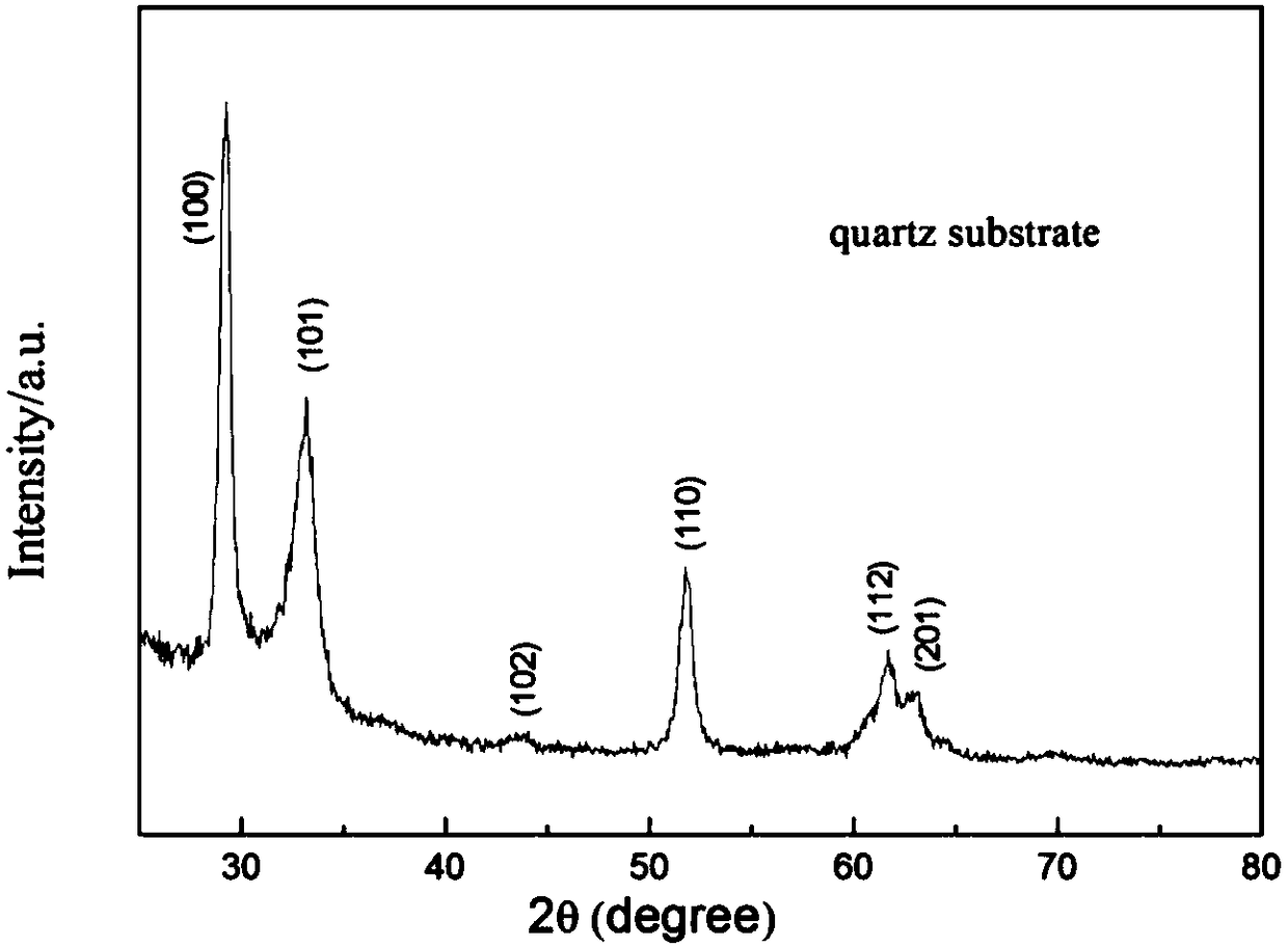
[0081] The XRD spectrum of the InN nanocrystalline film prepared on the quartz substrate in this embodiment is shown in image 3 ,from image 3 In the XRD analysis, it can be seen from the figure that there are obvious characteristic peaks, corresponding to (100), (101), (102), (110), (112) respectively, and the diffraction peaks are obvious, which is wurtzite The structure of the InN crystal, analyzed by Jade software, is consistent with the diffraction peak of the standard InN, indicating that the prepared InN nanocrystalline film has high crystal quality, high purity, and no impurity peaks.

[0082] The SEM image of the InN nanocrystalline film prepared on t...

Embodiment 3

[0084] A preparation device for non-polar indium nitride nanocrystalline thin film, same as embodiment 1.

[0085] A method for preparing a non-polar indium nitride nanocrystalline thin film, using the above-mentioned device, including the same steps as in Example 2, except that the temperature of the substrate sample stage is 450°C.

[0086] The SEM image of the InN nanocrystalline film prepared on the quartz substrate in this embodiment is shown in Figure 7 ,from Figure 7 , it can be seen that the prepared InN nanocrystalline thin film has uniform morphology and size, and is closely arranged on the quartz substrate.


PUM

PropertyMeasurementUnit
thicknessaaaaaaaaaa
lengthaaaaaaaaaa
distanceaaaaaaaaaa

Abstract

The invention relates to a device and a method for preparing a non-polar indium nitride nanocrystalline thin film, and belongs to the field of group III nitride optoelectronics. The device comprises areaction cavity, a substrate sample table, a beam source furnace, a radio frequency electrode, a vacuum mechanical pump, a molecular pump and a nitrogen supply system. The method comprises the following steps: cleaning a substrate and carrying out air drying, placing raw materials and the device according to requirements; carrying out vacuumizing, heating the sample table to 450-650 DEG C, and carrying out anneal for 10-30 minutes; closing the molecular pump, introducing 5-10sccm of nitrogen gas, and controlling the nitrogen pressure of the reaction cavity to be 25-50Pa; controlling the radiofrequency power to be 120-200W, and carrying out glow cleaning on the substrate; heating the beam source furnace to 700-800 DEG C, opening a metal baffle plate, maintaining the nitrogen flow rate, the nitrogen pressure of the reaction cavity and the radio frequency power unchanged, and carrying out a reaction for 3-5 hours; and closing the device, so as to obtain the non-polar indium nitride nanocrystalline thin film. The process method has the simple raw materials, low cost, and no catalyst or template, and the growth on a large-size substrate is facilitated.

Description

technical field [0001] The invention belongs to the technical field of III-nitride optoelectronics, and relates to a method for growing a III-nitride semiconductor thin film, in particular to a preparation device and method for a nonpolar indium nitride nanocrystal thin film. Background technique [0002] Indium Nitride (InN) is an important Group III nitride semiconductor material. Compared with AlN and GaN with wide bandgap, InN has a relatively narrow direct bandgap (0.7eV), small electronic effective mass, good Excellent properties such as steady-state and transient electrical transport characteristics, maximum electron mobility, etc. These special properties make InN have great application value in the field of optoelectronic devices such as high-frequency high-speed transistors, terahertz devices, chemical sensors, semiconductor light-emitting diodes, and full-spectrum solar cells. Since InN has low thermal stability and low decomposition temperature, ammonia as a nit...

Claims


Application Information

Patent Timeline
Patent Type & Authority Applications(China)
IPC IPC(8): C30B29/40C30B25/02
CPCC30B25/02C30B29/403
Inventor 沈龙海吕伟刘俊
Owner SHENYANG LIGONG UNIV
Why Eureka
Try Eureka