A kind of packaging film for flexible solar cell
A solar cell and encapsulation film technology, applied in circuits, electrical components, photovoltaic power generation, etc., can solve problems such as difficulty in maintaining adhesion, reduced efficiency of photovoltaic modules, and failure, so as to improve the ability to withstand ultraviolet aging and avoid migration And bleaching, to ensure long-term adhesion effect
- Summary
- Abstract
- Description
- Claims
- Application Information
AI Technical Summary
Problems solved by technology
Method used
Image
Examples
Embodiment 1
[0052] Preparation of gas barrier films
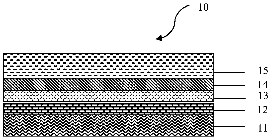
[0053] The first step: use a PET film with a thickness of 100 μm as the substrate, and coat a planarization layer with a thickness of 2 μm on its surface through a micro-gravure plate. The matrix resin of the planarization layer is a polyurethane-modified acrylic polymer;
[0054] Step 2: On the above-mentioned planarization layer, a silicon oxycarbide inorganic barrier layer is deposited using PECVD equipment, and the thickness of the inorganic barrier layer is 200 nm.
[0055] Preparation of adhesion-promoting layer:
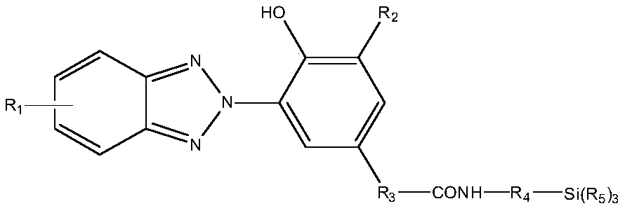
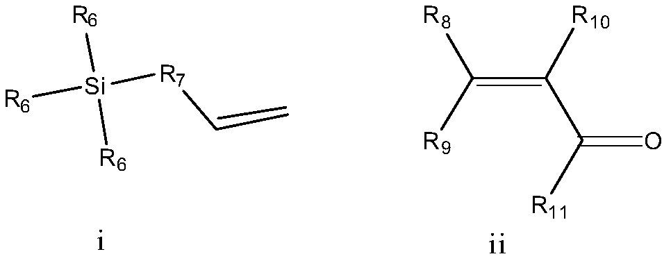
[0056] 500g of acryltrimethoxysilane and 500g of butyl acrylate were dissolved in 5kg of toluene, 50g of dibenzoyl peroxide was added, and reacted at 80°C for 24h under nitrogen protection to obtain a polymer with a number average molecular weight of 30,000, which was used as Component B1 is used. Dissolve 10g of A1 and 90g of B1 in 400g of toluene, add 1g of dibutyltin dilaurate, stir to dissolve and let it stand fo...
Embodiment 2
[0060] The process of gas barrier layer, tackifying layer and adhesive compounding is the same as that of Example 1, except that the weight ratio of A1 and B1 in the tackifying layer is 20:80.
[0061] The interlayer structure and the thickness of each layer of the encapsulation film are the same as in Example 1.
Embodiment 3
[0063] The process of gas barrier layer, tackifying layer and adhesive compounding is the same as that of Example 1, except that the weight ratio of A1 and B1 in the tackifying layer is 30:70. The interlayer structure and the thickness of each layer of the encapsulation film are the same as in Example 1.
PUM
| Property | Measurement | Unit |
|---|---|---|
| thickness | aaaaa | aaaaa |
| thickness | aaaaa | aaaaa |
| thickness | aaaaa | aaaaa |
Abstract
Description
Claims
Application Information


