Indium nitride nano column epitaxial wafer grown on aluminum foil substrate and preparation method thereof

A technology of nanocolumns and epitaxial wafers, which is applied in the direction of nanotechnology, nanotechnology, nanotechnology, etc. for materials and surface science, can solve the problems of inability to use epitaxial growth methods, obtain, etc., and achieve reduced defect density and high conductivity , the effect of uniform diameter

Active Publication Date: 2018-06-26
SOUTH CHINA UNIV OF TECH
View PDF4 Cites 9 Cited by
  • Summary
  • Abstract
  • Description
  • Claims
  • Application Information

AI Technical Summary

Problems solved by technology

[0006] In order to overcome the above-mentioned shortcomings and deficiencies of the prior art, the object of the present invention is to provide a kind of InN nano-column epitaxial wafer grown on the aluminum foil substrate, and the aluminum oxide amorphous layer on the surface of the aluminum foil substrate in the early stage of growth is subjected to highly active nitrogen plasma The bombardment effect of AlN forms the nucleation site of AlN on the surface of aluminum foil, which is helpful for the nucleation and further growth of InN nanocolumns, and solves the problem that the epitaxial growth method cannot be used to obtain vertical and uniform diameter InN nanocolumns on the aluminum foil substrate. At the same time, it can greatly reduce the defect density of the InN nanocolumn epitaxial layer, which can improve the radiative recombination efficiency of carriers, and can greatly improve the luminous efficiency of nitride devices such as semiconductor lasers and light-emitting diodes.

Method used


Image

  • Indium nitride nano column epitaxial wafer grown on aluminum foil substrate and preparation method thereof
  • Indium nitride nano column epitaxial wafer grown on aluminum foil substrate and preparation method thereof

Examples


Embodiment 1

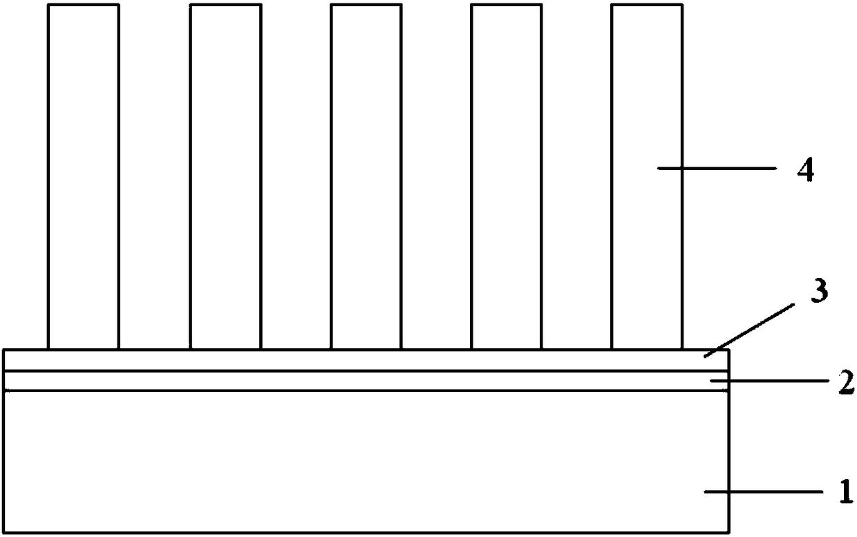
[0039] The InN nanocolumn epitaxial wafer grown on the aluminum foil substrate in this embodiment includes an aluminum foil substrate, an amorphous aluminum oxide layer, an AlN layer and an InN nanocolumn layer in sequence from bottom to top.

[0040] The preparation method of the InN nanocolumn epitaxial wafer grown on the aluminum foil substrate of the present embodiment comprises the following steps:

[0041] (1) Selection of substrate: use ordinary commercial aluminum foil substrate (the surface is oxidized);

[0042] (2) Substrate polishing and cleaning: The aluminum foil is mechanically polished and polished to obtain a flat surface; then the aluminum foil with a flat surface is placed in absolute ethanol for 1 minute to remove organic pollutants and sticky dirt on the surface of the aluminum foil substrate Particles, put them into deionized water and ultrasonic for 1 minute to remove surface impurities, and dry them with high-purity dry nitrogen;

[0043] (3) In-situ a...

Embodiment 2

[0049] The InN nanocolumn epitaxial wafer grown on the aluminum foil substrate in this embodiment includes an aluminum foil substrate, an amorphous alumina layer, an AlN layer and an InN nanocolumn layer in sequence from bottom to top. The InN nanocolumn layer takes AlN as the nucleation point, nucleates and grows the InN nanocolumn on the AlN.

[0050] The preparation method of the InN nanocolumn epitaxial wafer grown on the aluminum foil substrate of the present embodiment comprises the following steps:

[0051] (1) Selection of substrate and its crystal orientation: common commercial aluminum foil substrate is used;

[0052] (2) Substrate polishing and cleaning: Mechanically polish and polish the purchased common commercial aluminum foil to obtain a flat surface; then place the aluminum foil with a flat surface in absolute ethanol for 2 minutes to remove the organic matter on the surface of the aluminum foil substrate. Pollutants and sticky particles, put them into deioniz...


PUM

PropertyMeasurementUnit
thicknessaaaaaaaaaa
diameteraaaaaaaaaa

Abstract

The invention belongs to the technical field of nitride semiconductor devices and discloses an indium nitride nano column epitaxial wafer grown on an aluminum foil substrate and a preparation method thereof. An InN nano column epitaxial wafer grown on the aluminum foil substrate comprises an aluminum foil substrate, an amorphous aluminum oxide layer, an AlN layer and an InN nano column layer in sequence from bottom to top. The method comprises: 1, pretreating the surface-oxidized aluminum foil, and annealing in situ; 2, adopting a molecular beam epitaxial growth process, wherein the temperature of the substrate is from 400 to 700 DEG C, the pressure of the reaction chamber is from 4.0 to 10.0*10<-5> Torr, and the V / III beam ratio is from 20 to 40, growing the AlN nucleation points on the annealed aluminum foil substrate, and carrying out nucleation and growth of InN nano columns on the AlN. The nano columns of the invention are uniform in diameter and have high crystal quality. The defect density of an InN nano column epitaxial layer is greatly reduced, the radiation composite efficiency of carriers is improved, and the luminous efficiency of the nitride device is greatly improved.

Description

technical field [0001] The invention belongs to the technical field of nitride semiconductor devices, and relates to an indium nitride (InN) nano-column epitaxial wafer and a preparation method thereof, in particular to an InN nano-column epitaxial wafer grown on an aluminum foil substrate and a preparation method thereof. Background technique [0002] III-V nitrides are widely used in light-emitting diodes (LEDs), lasers, and optoelectronic devices due to their stable physical and chemical properties, high thermal conductivity, and high electron saturation velocity. Among III-V nitrides, indium nitride (InN) has attracted more and more attention from researchers due to its unique advantages. Among group III nitride semiconductors, InN has the smallest effective electron mass, the highest carrier mobility and the highest saturation transition velocity, which is extremely beneficial for the development of high-speed electronic devices. Not only that, InN has the smallest dir...

Claims


Application Information

Patent Timeline
Patent Type & Authority Applications(China)
IPC IPC(8): H01L21/02H01L33/32B82Y30/00B82Y40/00
CPCH01L33/32H01L21/02425H01L21/02458H01L21/02472H01L21/02502H01L21/0254H01L21/02631H01L21/02658B82Y30/00B82Y40/00H01L21/02488H01L21/02603H01L21/02645H01L29/0676H01L29/2003Y02P70/50
Inventor 高芳亮李国强张曙光温雷
Owner SOUTH CHINA UNIV OF TECH
Why Eureka
Try Eureka