Preparation method of micro-nano bending structure

A bending and micro-nano technology, applied in the field of micro-nano, can solve problems such as poor orientation of structural space, inability to meet the needs of scientific research and processing, high time and cost costs, etc., to achieve flexible controllability, clear processing mechanism and formation principle , the effect of large preparation area

Inactive Publication Date: 2018-06-29
INST OF PHYSICS - CHINESE ACAD OF SCI
View PDF8 Cites 9 Cited by
  • Summary
  • Abstract
  • Description
  • Claims
  • Application Information

AI Technical Summary

Problems solved by technology

Although these approaches can form three-dimensional structures, there are some problems in these methods. For example, the usual dry or wet etching process has high requirements on the substrate, and is selective for materials, and cannot be processed flexibly. structure, and the spatial orientation difference of the structure, etc.
However, the manual folding method is difficult to achieve three-dimensional structure processing on the order of microns and nanometers, and at the same time requires high time and cost.
With the continuous expansion of the demand for micro-nano-scale three-dimensional structures, the above methods can no longer meet the needs of current scientific research and processing.

Method used


Image

  • Preparation method of micro-nano bending structure
  • Preparation method of micro-nano bending structure
  • Preparation method of micro-nano bending structure

Examples


preparation example Construction

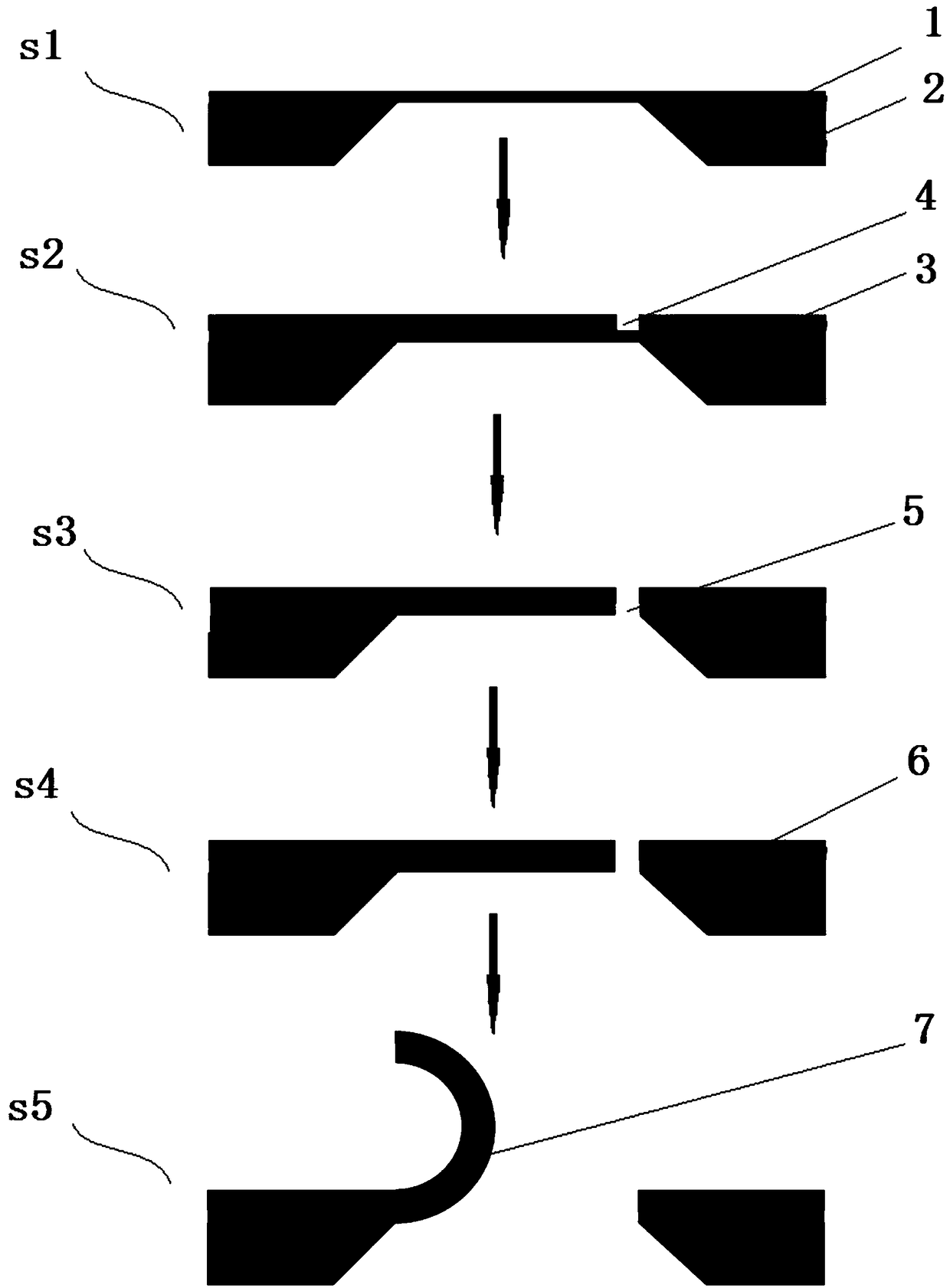
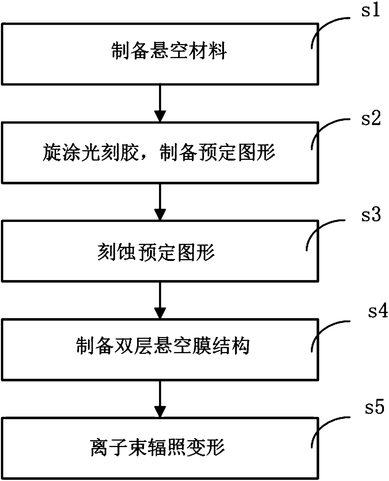
[0031] figure 1 It is a schematic diagram of the fabrication process of a fabrication method of a micro-nano curved structure according to an embodiment of the present invention. figure 2 It is a schematic flowchart of a method for preparing a micro-nano curved structure according to an embodiment of the present invention. Such as figure 1 and figure 2 As shown, the preparation method of a micro-nano curved structure provided by the present invention is to introduce a stress change to make it bend by irradiating the surface of the suspended double-layer film, and then control the shape of the two-dimensional film by changing the irradiation energy. The degree of bending specifically includes the following steps:

[0032] s1. Prepare the suspended material 1 on the substrate 2;

[0033] s2. Spin-coat photoresist 3 on the suspended material 1, and prepare predetermined pattern 4 by exposing photoresist 3;

[0034] s3, transfer the predetermined pattern 4 to the suspended ...

Embodiment 1

[0046] Step 1: Purchase a commercial 20nm silica window and clean it under oxygen plasma for 20 seconds;

[0047] Step 2: Spin-coat electron beam photoresist PMMA on the purchased silicon substrate at a speed of 4000r / min, and then place it on a 180°C hot plate and bake for 1min;

[0048] Step 3: Use the electron beam exposure process to expose the sample obtained in step 2. The exposed pattern is set as the inverse pattern of the stripe pattern, and the PMMA developer is used for development, and the unmasked parts are removed by reactive ion etching. Silica Graphics;

[0049] Step 4: Remove the photoresist PMMA from the sample obtained in step 3 by oxygen plasma etching, and deposit 40 nanometers of gold by thermal evaporation process;

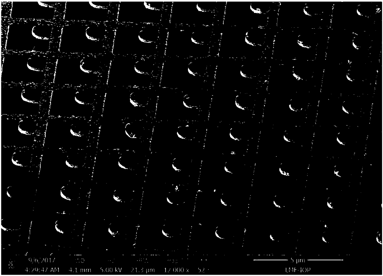
[0050] Step 5: The sample obtained in step 4 is placed under the ion beam generated by reactive ion etching, and the sample is treated with oxygen plasma to obtain a three-dimensional curved structure.

[0051] The pattern of the three-dim...

Embodiment 2

[0053] Step 1: Deposit 100 nanometers of Au on a clean silicon wafer coated with a sacrificial layer by electron beam deposition, and transfer the gold film to a copper grid for TEM in an acetone environment to obtain a suspended gold window;

[0054] Step 2: Spin-coat UV photoresist S1813 on the transferred gold window at a speed of 3000r / min, and then bake on a hot plate at 115°C for 1min;

[0055] Step 3: Use the electron beam exposure process to expose the sample obtained in step 2. The exposed pattern is set as the inverse pattern of the "T" pattern, develop with S1813 developer, and use ion milling to remove the unmasked gold. graphics;

[0056] Step 4: Use acetone to remove the photoresist S1813 from the sample obtained in step 3; use pulsed laser deposition process to deposit TiO 2 40 nanometers;

[0057] Step 5: Place the sample obtained in step 4 under ion milling, and irradiate the sample with argon plasma to obtain a three-dimensional curved structure.


PUM

PropertyMeasurementUnit
thicknessaaaaaaaaaa

Abstract

The invention provides a preparation method of a micro-nano bending structure, and belongs to the field of nanotechnologies. The method comprises the steps of preparing a suspending material on a substrate; rotationally coating photoresist on the suspending material, and preparing a predetermined pattern through exposing the photoresist; transferring the predetermined pattern to the suspending material through etching; removing the photoresist, and performing material deposition on the suspending material to acquire a dual-layer suspending film structure of the suspending material and the deposited material; and irradiating the dual-layer suspending film structure with ion beams to deform, so as to acquire the micro-nano bending structure. According to the preparation method of the micro-nano bending structure provided by the invention, the limitations of three-dimensional processing methods such as folding on the machining of large area and hundred-nanometer structure scales and on the flexibility of the structure space can be broken, and thus the three-dimensional machining method which is flexible and strong in controllability is acquired.

Description

technical field [0001] The invention relates to the field of micro-nano technology, in particular to a method for preparing a micro-nano curved structure. Background technique [0002] With the development of electronic devices and optical devices, three-dimensional curved structures have been increasingly used in the devices we use. For example, in optical metamaterials, two-dimensional or planar optical metamaterials are difficult to couple with the magnetic field component of light, so in many cases they cannot give full play to the control advantages of optical metamaterials, while three-dimensional optical metamaterials are not suitable for light. Incidence can then respond to its magnetic field component. Three-dimensional metamaterials are a good way to obtain the response of metamaterials to the magnetic component of light. When making electronic devices, three-dimensional electronic devices have a smaller volume, so higher integration can be obtained, and at the s...

Claims


Application Information

Patent Timeline
Patent Type & Authority Applications(China)
IPC IPC(8): B81C1/00
CPCB81C1/0015B81C1/00182B81C1/00349B81C1/00555
Inventor 李俊杰潘如豪顾长志刘哲金爱子田士兵
Owner INST OF PHYSICS - CHINESE ACAD OF SCI
Why Eureka
Try Eureka