Low-drive-voltage lithium niobateelectrooptical modulator and manufacturing method thereof

An electro-optical modulator, low driving voltage technology, applied in the fields of instruments, optics, nonlinear optics, etc., can solve the problems of increasing the driving voltage of the modulator, the modulation efficiency is not high, increasing the driving voltage of the electro-optical modulator, etc., to reduce the driving voltage. , the effect of improving the modulation efficiency

Pending Publication Date: 2018-07-03
天津领芯科技发展有限公司
View PDF0 Cites 8 Cited by
  • Summary
  • Abstract
  • Description
  • Claims
  • Application Information

AI Technical Summary

Problems solved by technology

[0005] (1) The lithium niobate electro-optic modulator adopts a coplanar electrode structure, and the modulation efficiency of the electric field loaded on the coplanar electrode structure to the optical field is not high, which increases the driving voltage of the modulator;
[0006] (2) In order to realize the improvement of operating frequency or bandwidth of lithium niobate electro-optic modulators, especially high-frequency electro-optic modulators, it is often necessary to prepare a layer of silicon dioxide film with a thickness of 0.2 μm to 2 μm on the surface of lithium niobate as a buffer layer to reduce the effective refractive index of the microwav

Method used


Image

  • Low-drive-voltage lithium niobateelectrooptical modulator and manufacturing method thereof
  • Low-drive-voltage lithium niobateelectrooptical modulator and manufacturing method thereof
  • Low-drive-voltage lithium niobateelectrooptical modulator and manufacturing method thereof

Examples


Embodiment 1

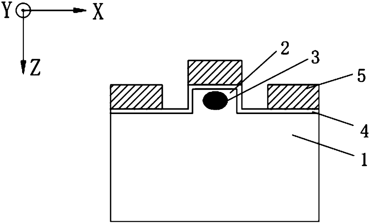
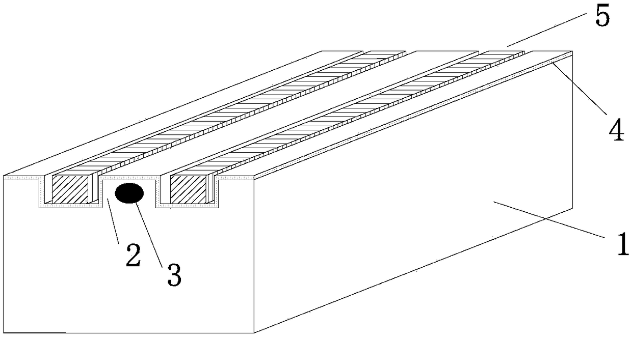
[0088] figure 2 and image 3 It is the first embodiment of the low driving voltage lithium niobate electro-optic modulator proposed by the present invention, which is a high modulation bandwidth (or high modulation rate) lithium niobate phase modulator. For lithium niobate electro-optic modulators with high modulation bandwidth (or high modulation rate), traveling wave electrode structure is often used, and silicon dioxide film is often added as a buffer layer to achieve speed matching and impedance matching, and improve device modulation bandwidth ( or modulation rate).

[0089] The lithium niobate electro-optic modulator provided in this embodiment includes: a lithium niobate wafer 1 , a ridge structure 2 , an optical waveguide 3 , a silicon dioxide film 4 , and a modulation electrode 5 .

[0090] The lithium niobate wafer 1 is a lithium niobate single crystal material, the tangential direction of the crystal is X-cut and Y-cut, and the thickness is 0.1 mm to 2 mm.

[00...

Embodiment 2

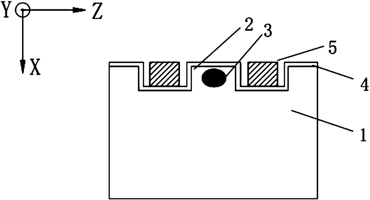
[0103] Figure 4 and Figure 5 It is the second embodiment of the low driving voltage lithium niobate electro-optic modulator proposed by the present invention, which is a high modulation bandwidth (or high modulation rate) lithium niobate intensity modulator. For lithium niobate electro-optic modulators with high modulation bandwidth (or high modulation rate), traveling wave electrode structure is often used, and silicon dioxide film is often added as a buffer layer to achieve speed matching and impedance matching, and improve device modulation bandwidth ( or modulation rate).

[0104] The lithium niobate electro-optic modulator provided in this embodiment includes: a lithium niobate wafer 1 , a ridge structure 2 , an optical waveguide 3 , a silicon dioxide film 4 , and a modulation electrode 5 .

[0105] The lithium niobate wafer 1 is a lithium niobate single crystal material, the tangential direction of the crystal is X-cut and Y-cut, and the thickness is 0.1 mm to 2 mm. ...

Embodiment 3

[0118] Figure 6 and Figure 7 It is the third embodiment of the low driving voltage lithium niobate electro-optic modulator proposed by the present invention, which is a phase modulator with high modulation bandwidth (or high modulation rate) based on lithium niobate thin film. By thinning the lithium niobate wafer and making the lithium niobate thin film on the low dielectric constant substrate wafer, it is beneficial to improve the modulation bandwidth (or modulation rate) of the lithium niobate electro-optic modulator, and the lithium niobate thin film is made The ridge structure is beneficial to reduce the driving voltage of the device while maintaining the high modulation bandwidth (or high modulation rate) of the lithium niobate electro-optic modulator provided in this embodiment.

[0119] The lithium niobate electro-optic modulator provided in this embodiment includes: a base wafer 6 , a lithium niobate thin film 7 , a ridge structure 2 , an optical waveguide 3 , and ...


PUM

PropertyMeasurementUnit
Thicknessaaaaaaaaaa
Widthaaaaaaaaaa
Heightaaaaaaaaaa

Abstract

The invention discloses a low-drive-voltage lithium niobateelectrooptical modulator. A ridge waveguide structure is made on an X-cut Y-pass lithium niobate crystal, and the electrode structures of theelectrooptical modulator are made on two sides of the ridge waveguide structure, so that the electric field between the electrode structures of the electrooptical modulator can be distributed along the horizontal direction. Compared with existing lithium niobateelectrooptical modulator, the lithium niobateelectrooptical modulator disclosed by the invention has the advantages that the modulation efficiency of an optical field can be remarkably improved by an electric field, and the drive voltage of a device is reduced. In other schemes, a low-dielectric-constant material can be adopted as a substrate wafer of a lithium niobate film, and the ridge waveguide structure is made on the lithium niobate film, thus the working bandwidth of the lithium niobateelectrooptical modulator can be effectively increased, and the drive voltage of the lithium niobateelectrooptical modulator can be lowered. The invention also provides a manufacturing method of the low-drive-voltage lithium niobateelectrooptical modulator.

Description

technical field [0001] The invention relates to the technical fields of optical fiber communication, coherent optical communication and microwave photonics, in particular to a low driving voltage lithium niobate electro-optical modulator and a manufacturing method thereof. Background technique [0002] The electro-optic modulator is one of the core devices in the optical fiber communication system, and it plays a key role in converting electrical signals to optical signals. With the continuous development of communication technology, the technology of using ultra-low loss optical fiber as the information transmission medium has also been applied to the technical fields of coherent optical communication and microwave photonics. [0003] In optical fiber communication, especially in coherent optical communication systems, the optical modules used are developing in the direction of low power consumption, and the reduction of power consumption of optical modules will inevitably ...

Claims


Application Information

Patent Timeline
IPC IPC(8): G02F1/03G02F1/035
CPCG02F1/0311G02F1/035
Inventor 李萍范宝泉尚含予
Owner 天津领芯科技发展有限公司
Why Eureka
Try Eureka