Preparation method of high k-gate dielectric layer and silicon carbide MOS power device

A gate dielectric layer and power device technology, applied in semiconductor devices, semiconductor/solid-state device manufacturing, electrical components, etc., can solve problems such as uneven oxide layer thickness, high electric field strength, etc., to improve channel mobility, improve resistance Compression ability, effect of reducing impurity content

Active Publication Date: 2018-07-06
GLOBAL ENERGY INTERCONNECTION RES INST CO LTD +2
View PDF9 Cites 5 Cited by
  • Summary
  • Abstract
  • Description
  • Claims
  • Application Information

AI Technical Summary

Problems solved by technology

[0005] 2. The crystal lattice of silicon carbide has anisotropic characteristics, and its oxidation rate has strong anisotropy, which leads to the problem of uneven thickness of the oxide layer on different crystal planes;
[0006] 3. SiO 2 The dielectric constant K of the dielectric material OX The value is only 3.9, making SiC / SiO 2 SiO in the interface electric field intensity distribution 2 A higher electric field strength will appear on the side, thereby limiting the high breakdown electric field strength of SiC

Method used


Image

  • Preparation method of high k-gate dielectric layer and silicon carbide MOS power device
  • Preparation method of high k-gate dielectric layer and silicon carbide MOS power device
  • Preparation method of high k-gate dielectric layer and silicon carbide MOS power device

Examples


Embodiment 1

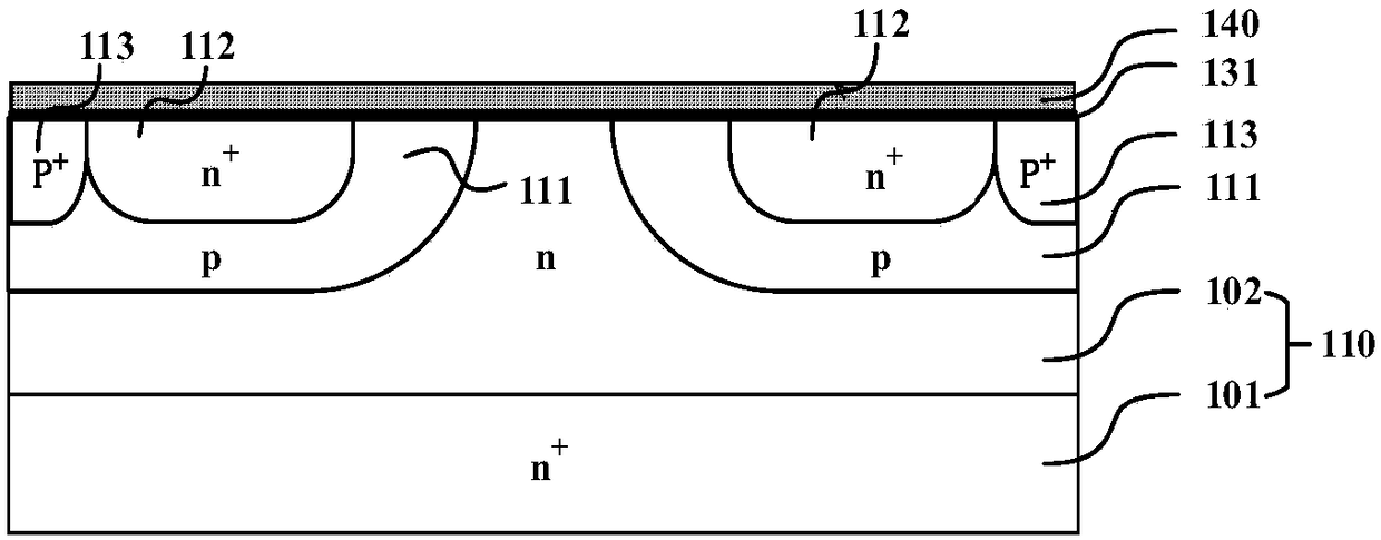
[0074] Step S201: Prepare silicon carbide epitaxial wafer

[0075] figure 2 It is a schematic structural diagram of a silicon carbide epitaxial wafer in an embodiment of the present invention. As shown in the figure, a silicon carbide epitaxial wafer 110 in this embodiment includes an n-type silicon carbide substrate 101 and an n-type silicon carbide epitaxial layer 102 .

[0076] Step S202: Prepare well region, source contact region and base contact region

[0077] image 3 It is a schematic diagram of the well region, the source contact region and the base contact region of a silicon carbide epitaxial wafer in an embodiment of the present invention. The p-type well region 111 is doped with p-type ions and n-type ions respectively to form an n-type base contact region 112 and a p-type source contact region 113 .

[0078] Step S203: preparing a sacrificial oxide layer

[0079] Figure 4 It is a schematic diagram of a sacrificial oxide layer of a silicon carbide epitaxial...

Embodiment 2

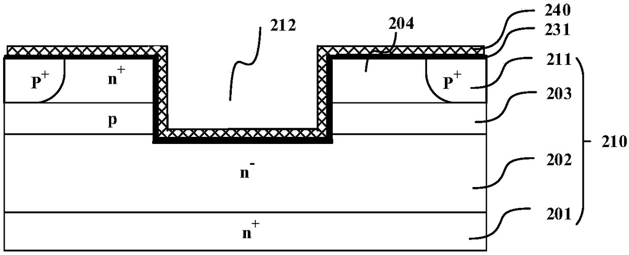
[0087] Step S301: Prepare silicon carbide epitaxial wafer

[0088] Figure 9 It is a schematic structural diagram of another silicon carbide epitaxial wafer in the embodiment of the present invention. As shown in the figure, the silicon carbide epitaxial wafer 210 in this embodiment includes an n-type silicon carbide substrate 201, an n-type silicon carbide epitaxial layer 202, and a p-type silicon carbide epitaxial layer 202. SiC epitaxial layer 203 and n-type SiC epitaxial layer 204 .

[0089] Step S302: Prepare base contact region and trench region

[0090] Figure 10 It is a schematic diagram of the base contact region and trench region of another silicon carbide epitaxial wafer in the embodiment of the present invention. As shown in the figure, in this embodiment, the n-type silicon carbide epitaxial layer 204 is doped with p-type ions to form the base contact In the region 211 , the n-type silicon carbide epitaxial layer 202 , the p-type silicon carbide epitaxial laye...

Embodiment 3

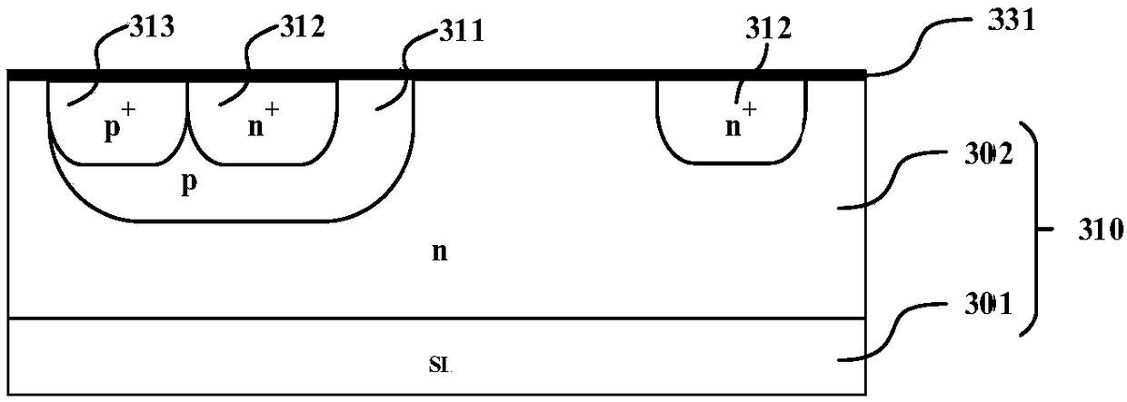
[0100] Step S401: Prepare silicon carbide epitaxial wafer

[0101] Figure 16 It is a schematic structural diagram of another silicon carbide epitaxial wafer in the embodiment of the present invention. As shown in the figure, the silicon carbide epitaxial wafer 310 in this embodiment includes an n-type silicon carbide substrate 301 and a semi-insulating silicon carbide substrate 302 .

[0102] Step S402: Prepare well region, source contact region and base contact region

[0103] Figure 17 It is a schematic diagram of the well region, the source contact region and the base contact region of another silicon carbide epitaxial wafer in the embodiment of the present invention. As shown in the figure, the n-type silicon carbide epitaxial layer 302 is doped with p-type ions in this embodiment A p-type well region 311 is formed, and p-type ions and n-type ions are respectively doped in the p-type well region 311 to form an n-type base contact region 312 and a p-type source contact ...


PUM

PropertyMeasurementUnit
thicknessaaaaaaaaaa
electrical resistivityaaaaaaaaaa

Abstract

The present invention provides a preparation method of a high k-gate dielectric layer and a silicon carbide MOS power device. The preparation method comprises the steps of: performing high-temperaturesacrificial oxidation of a silicon carbide epitaxial wafer with a first conductive type, and forming a sacrificial oxidation layer at the upper surface of the epitaxial layer of the silicon carbide epitaxial wafer; performing corrosion of the sacrificial oxidation layer until the sacrificial oxidation layer on the epitaxial layer is completely removed; performing high-temperature surfacing processing of the upper surface of the epitaxial layer after removal of the sacrificial oxidation layer, and forming a smooth passivated surface; and depositing an Al2O3 dielectric coating layer, a LaAlO3 dielectric layer and an Al2O3 dielectric coating layer at the smooth passivated surface in order, performing annealing of a laminated structure formed by the Al2O3 dielectric coating layer, the LaAlO3dielectric layer and the Al2O3 dielectric coating layer, and forming a high k-gate dielectric layer. Compared to the prior art, the preparation method of the high k-gate dielectric layer and the silicon carbide MOS power device can reduce the interface defects caused by impurities and/or surface lattice defects at a SiC/SiO2 interface so as to improve the voltage endurance capability of the gate dielectric layer.

Description

technical field [0001] The invention relates to the technical field of semiconductor devices, in particular to a method for preparing a high-k gate dielectric layer and a silicon carbide MOS power device. Background technique [0002] Silicon carbide semiconductor material has a wide band gap (3.2eV), a high breakdown electric field strength (2.2MV / cm), a high high saturation electron mobility (2.0×10 7 cm / s), high thermal conductivity (5.0W / cm K), excellent physical and chemical stability and other characteristics, suitable for the manufacture of high power, high voltage, high operating temperature, high operating frequency power semiconductor devices material, and since silicon carbide is the only compound semiconductor material that has the ability to generate dense SiO through oxidation 2 The ability of the dielectric layer, which makes the silicon carbide process and the conventional CMOS process have higher process compatibility and maturity, and also makes the silico...

Claims


Application Information

Patent Timeline
Patent Type & Authority Applications(China)
IPC IPC(8): H01L21/04H01L29/51H01L29/78
CPCH01L21/049H01L29/513H01L29/517H01L29/78
Inventor 夏经华杨霏郑柳焦倩倩查祎英李永平田亮张文婷李嘉琳
Owner GLOBAL ENERGY INTERCONNECTION RES INST CO LTD
Why Eureka
Try Eureka