Z-shaped semiconductor photocatalyst with trapezoid structure as well as preparation method and application thereof

A trapezoidal structure and photocatalyst technology, applied in the field of photocatalysis, can solve the problems of easy recombination and less semiconductor catalysts, and achieve the effects of stable properties, improved efficiency and improved efficiency.

Active Publication Date: 2018-07-13
LIAONING UNIVERSITY
View PDF7 Cites 4 Cited by
  • Summary
  • Abstract
  • Description
  • Claims
  • Application Information

AI Technical Summary

Problems solved by technology

However, if it is to be carried out at the same time, a problem with this semiconductor photocatalytic technology is that photogenerated electrons and hole pairs are easy to recombine.
The photocatalytic system must carry out both oxida...

Method used


Image

  • Z-shaped semiconductor photocatalyst with trapezoid structure as well as preparation method and application thereof
  • Z-shaped semiconductor photocatalyst with trapezoid structure as well as preparation method and application thereof
  • Z-shaped semiconductor photocatalyst with trapezoid structure as well as preparation method and application thereof

Examples


Embodiment 1

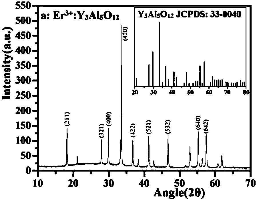
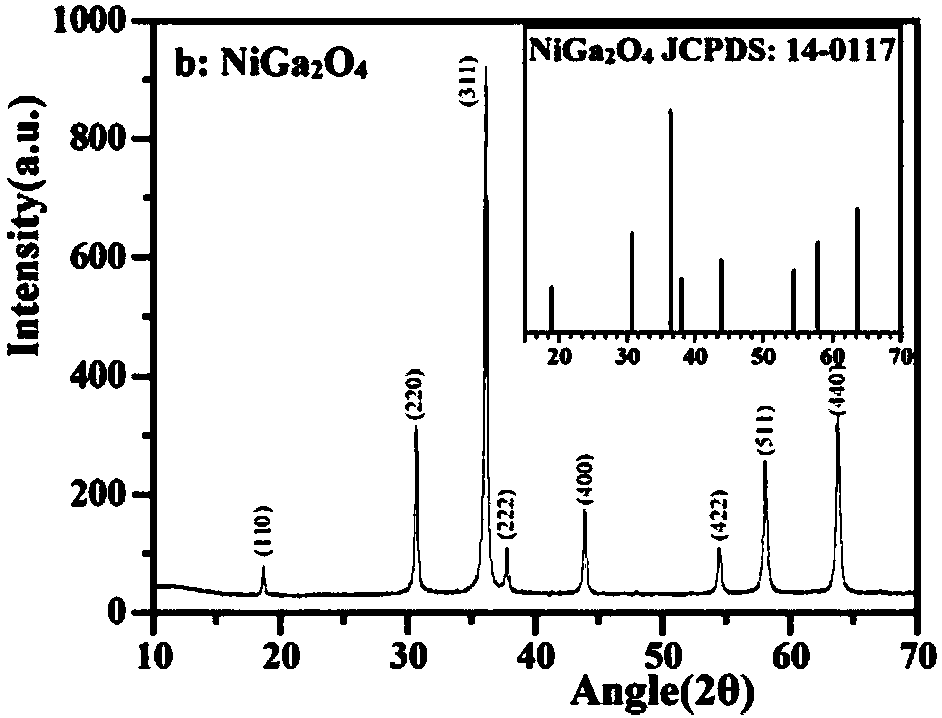
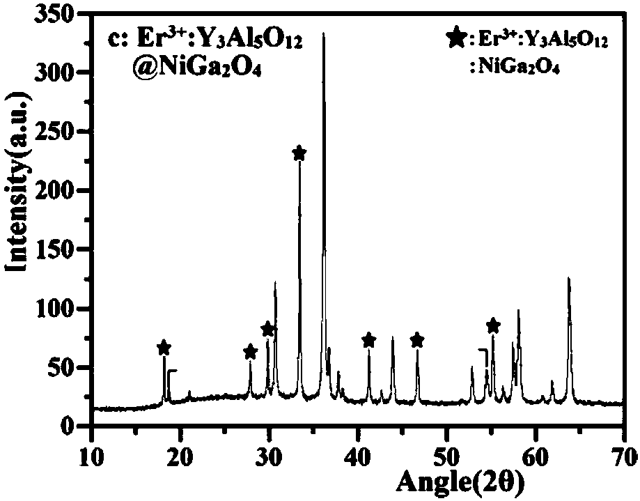
[0030] Embodiment 1 has the Z-type semiconductor photocatalyst Er of trapezoidal structure 3+ :Y 3 al 5 o 12 @NiGa 2 o 4 / NiS / Bi 2 sn 2 o 7

[0031] (1) Preparation of NiGa 2 o4 nano powder

[0032] 0.376g Ga 2 o 3 The powder was added to 50 mL of 1mol / L nickel nitrate solution, and the resulting mixture was adjusted to pH 12 with sodium hydroxide (stirring for 30 min while adjusting), and the resulting suspension solution was transferred to a reactor at 180°C for 48 h, cooled to room temperature, A light blue precipitate was obtained, washed several times with deionized water, and then dried at 60°C for 8 hours to obtain NiGa 2 o 4 Powder. Grind the powder finely, bake it in a muffle furnace at 500°C for 2 hours, take it out, and then grind it to get NiGa 2 o 4 Nano powder.

[0033] (2) Preparation of Bi 2 sn 2 o 7 nano powder

[0034] 8.76g Bi(NO 3 ) 3 ·5H 2 O and 5.40 g K 2 SnO 3 ·3H 2 O was mixed in 150ml deionized water, and adjusted to PH=12 wi...

Embodiment 2

[0054] Example 2 Er 3+ :Y 3 Al 5 o 12 @NiGa 2 o 4 / NiS / Bi 2 sn 2 o 7 Application in photocatalytic conversion of nitrite and sulfite

[0055] (1) Effect of simulated sunlight irradiation time and corresponding reaction kinetics on the photocatalytic conversion rate of nitrite and sulfite

[0056] Perform Er under simulated sunlight 3+ :Y 3 Al 5 o 12 @NiGa 2 o 4 / NiS / Bi 2 sn 2 o 7 Photocatalytic conversion of nitrite and sulfite by photocatalysts. Before light exposure, will contain NO 2 - and SO 3 2- The solution was stirred for 30 min in the dark and reached adsorption-desorption equilibrium. Then, solution samples were taken every 1.0 hour, and the conversion of nitrite and sulfite was checked by ion chromatography. From Figure 5a It can be seen that with the increase of the simulated sunlight irradiation time, the photocatalytic conversion rate shows an upward trend. Under irradiation within 4.00 hours, for NO 2 - and SO 3 2- , and their photoc...


PUM

PropertyMeasurementUnit
Diameteraaaaaaaaaa

Abstract

The invention relates to a Z-shaped semiconductor photocatalyst with a trapezoid structure as well as a preparation method and application thereof. The Z-shaped semiconductor photocatalyst is preparedthrough a sol-gel method, a hydrothermal method and a high-temperature calcination method; a narrow band gap semiconductor is embedded between Er<3+>:Y3Al5O12@NiGa2O4 and Bi2Sn2O7 and is used as a good conductor as a conductive ladder to form the Z-shaped semiconductor photocatalyst Er<3+>:Y3Al5O12@NiGa2O4/NiS/Bi2Sn2O7 with the trapezoid structure; the composite material has highly-stable photocatalytic activity in nitrite and sulfite conversion processes; the conversion rates of nitrite and sulfite reach 86.23 percent to 94.44 percent respectively under the irradiation of simulated sunlight.The photocatalyst with the Z-shaped structure has stable and efficient photocatalytic activity and has a wide application prospect in nitrite and sulfite wastewater treatment.

Description

technical field [0001] The invention belongs to the field of photocatalysis, in particular to a Z-type semiconductor photocatalyst Er with a trapezoidal structure similar to "a conduction elevator". 3+ :Y 3 al 5 o 12 @NiGa 2 o 4 / NiS / Bi 2 sn 2 o 7 Its preparation method and application in photocatalytic conversion of nitrite and sulfite. Background technique [0002] Water is indispensable for human life and production activities. In modern life, due to industrial wastewater and domestic sewage flowing into rivers and lakes, water pollution is serious. Water pollution directly endangers human health and has a huge negative impact on social life. Among them, the pollution of nitrite and sulfite in surface water and groundwater has been very serious. This urgent pollution crisis has captured the attention of the world. Nitrite can be used as food colorant and preservative, mainly from food industry wastewater. Groundwater containing high concentrations of nitrite ...

Claims


Application Information

Patent Timeline
IPC IPC(8): B01J27/043C02F1/30C02F101/16C02F101/10
CPCB01J27/043B01J35/004C02F1/30C02F2101/101C02F2101/166C02F2305/10
Inventor 马雪王国伟王春权宋有涛王君
Owner LIAONING UNIVERSITY
Why Eureka
Try Eureka