Hemt epitaxial structure with multi-quantum well high-resistance buffer layer and preparation method

A high-resistance buffer layer, multi-quantum well layer technology, applied in semiconductor/solid-state device manufacturing, semiconductor devices, electrical components, etc., can solve the problems of contaminating the reaction chamber, affecting device characteristics, and decreasing the channel 2DEG mobility, etc. To achieve the effect of strong controllability and simple production method

Active Publication Date: 2020-08-25
HUNAN SANAN SEMICON CO LTD
View PDF6 Cites 0 Cited by
  • Summary
  • Abstract
  • Description
  • Claims
  • Application Information

AI Technical Summary

Problems solved by technology

Generally, there are two ways to obtain high-resistance GaN-based epitaxial materials: one is to increase the p- Type impurity or defect energy level compensation background electron concentration to obtain a high resistance GaN layer; another method is to form deep energy level defects or provide holes to compensate the remaining Carriers to obtain a high-resistance GaN layer; the first method is to obtain a high-resistance GaN epitaxial layer by introducing defect impurities, so the quality of the epitaxial layer will deteriorate, and at the same time obtain a high-resistance GaN method by controlling the growth conditions. The device dependence is strong, and the repeatability is poor; the second method introduces metal impurities that have a memory effect and will pollute the reaction chamber. An MOCVD is required to grow high-resistance GaN, and the introduction of impurities will reduce the mobility of the channel 2DEG , affecting the device characteristics

Method used


Image

  • Hemt epitaxial structure with multi-quantum well high-resistance buffer layer and preparation method
  • Hemt epitaxial structure with multi-quantum well high-resistance buffer layer and preparation method
  • Hemt epitaxial structure with multi-quantum well high-resistance buffer layer and preparation method

Examples


Embodiment 1

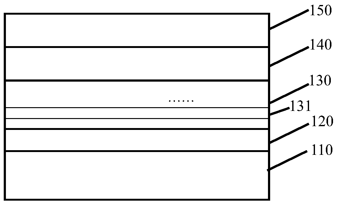
[0050] refer to figure 1 , using p-i-n multiple quantum wells as a high-resistance buffer layer for GaN back barriers on SiC substrates

[0051] (1) An AlN nucleation layer 120 is grown on a 500um 6-inch silicon carbide substrate 110 by MOCVD. Desorption at a high temperature of 1050°C for 10 minutes removes oxides and impurities on the SiC surface, revealing a stepped surface morphology. Then grow the nucleation layer 120 at a high temperature: the growth temperature is 1100° C., the TMAl flow rate is 250 sccm, and the NH 3 The flow rate is 3000sccm, the pressure in the reaction chamber is 70mbar, the growth rate is about 0.3um / h, and the growth time is 30min. The thickness of the AlN nucleation layer 120 is about 150nm;

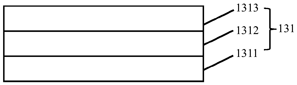
[0052] (2) Continue to grow the p-i-n multi-quantum well layer 130 with an average Al composition of about 5% on the AlN nucleation layer 120 in (1) by MOCVD as the back barrier layer. refer to figure 2 , p-i-n multi-quantum well layer 130 growth incl...

Embodiment 2

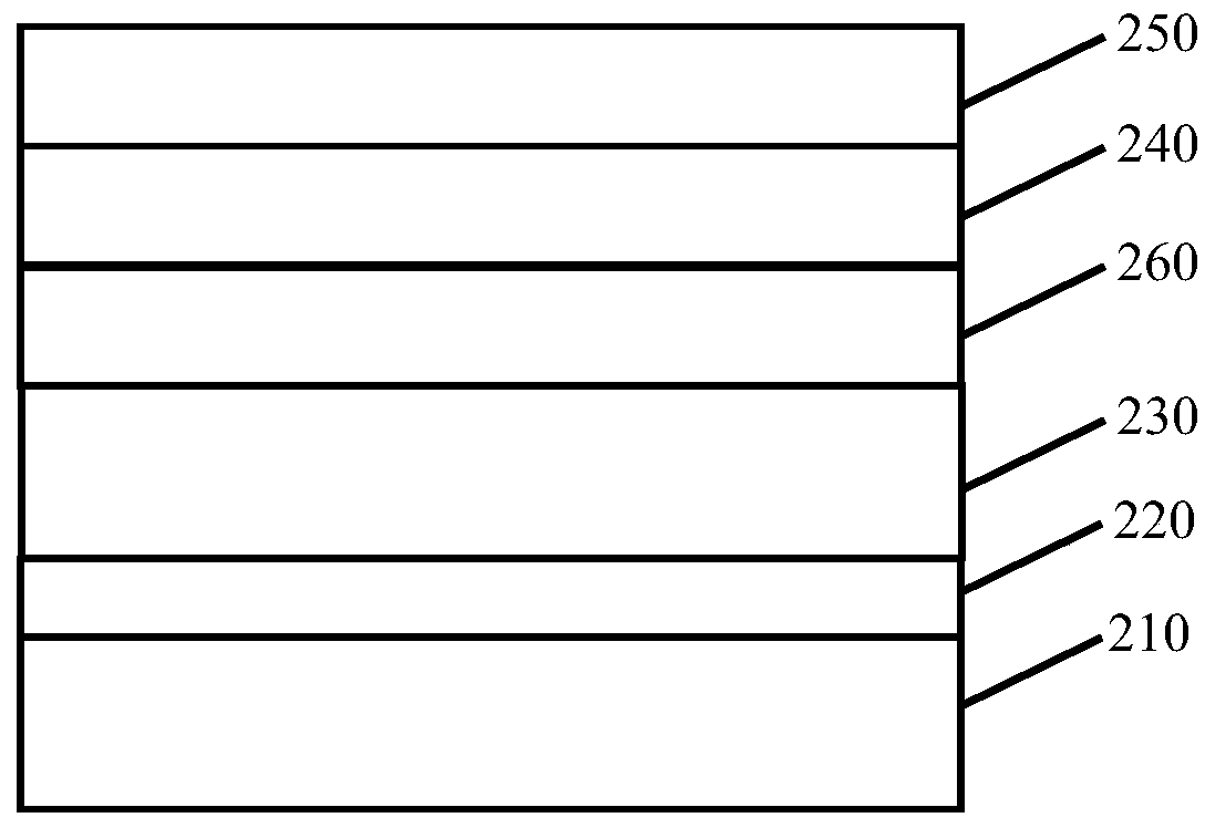
[0056] refer to image 3 , using p-i-n multiple quantum wells as a high-resistance buffer layer for GaN epitaxial stress transfer on Si substrates

[0057] (1) An AlN nucleation layer 220 is grown on a 1mm 6-inch silicon substrate 210 by MOCVD. Desorption at a high temperature of 1050°C for 15 minutes removes oxides and impurities on the Si surface, revealing a stepped surface morphology. Then grow the nucleation layer 220 at high temperature: the growth temperature is 1100° C., the TMAl flow rate is 250 sccm, the NH 3 The flow rate is 3000sccm, the pressure in the reaction chamber is 70mbar, the growth rate is about 0.3um / h, and the growth time is 40min. The thickness of the AlN nucleation layer 220 is about 200nm.

[0058] (2) Continue to grow p-i-n multi-quantum well layer 230 with an average Al composition of about 20% on the AlN nucleation layer 220 in (1) by MOCVD as a high-resistance stress transfer layer. The growth of the p-i-n multi-quantum well layer 230 include...

Embodiment 3

[0063] refer to Figure 4 , using p-i-n multiple quantum wells with graded Al composition as a high-resistance buffer layer for GaN epitaxial stress transfer on Si substrates

[0064] (1) An AlN nucleation layer 320 is grown on a 1mm 6-inch silicon substrate 310 by MOCVD. Desorption at a high temperature of 1050°C for 15 minutes removes oxides and impurities on the Si surface, revealing a stepped surface morphology. Then grow the nucleation layer 320 at high temperature: the growth temperature is 1100° C., the flow rate of TMAl is 250 sccm, the flow rate of NH3 is 3000 sccm, the pressure of the reaction chamber is 70 mbar, the growth rate is about 0.3 um / h, and the growth time is 40 min. The thickness of the AlN nucleation layer 320 is about 200nm.

[0065] (2) Continue to grow p-i-n multi-quantum well layer 330 with an average Al composition of about 72.5% on the AlN nucleation layer 320 of (1) by MOCVD as a high-resistance stress transfer layer. The growth of the p-i-n mu...


PUM

PropertyMeasurementUnit
thicknessaaaaaaaaaa
thicknessaaaaaaaaaa
thicknessaaaaaaaaaa

Abstract

The invention discloses a high electron mobility field effect transistor (HEMT) epitaxial structure and a method thereof prepared by growing a p-i-n multi-quantum well heterojunction and having a high-resistance GaN-based buffer layer. Taking advantage of the large difference between the spontaneous polarization intensities of AlN and GaN, polarized doping is achieved by growing AlGaN with a graded Al composition to obtain p-type Al x Ga 1‑x N-layer and n-type Al z Ga 1‑z N layer and fixed component Al by high temperature growth y Ga 1‑y N layer, so as to obtain a p-i-n multi-quantum well heterojunction, in the p-i-n heterojunction, due to the existence of the built-in electric field, the i layer is a completely depleted region, thereby obtaining a low-carrier concentration The high-resistance GaN-based buffer layer can effectively reduce the leakage current of the buffer layer, and at the same time improve the crystal quality of the epitaxial material to improve the high-voltage characteristics of the device and reduce the useless power consumption of the device, which is suitable for practical production applications.

Description

technical field [0001] The invention relates to semiconductor material growth and epitaxial growth of device structure layers, in particular to a HEMT epitaxial structure and method with a high-resistance GaN-based buffer layer prepared by p-i-n multi-quantum well heterojunction. Background technique [0002] GaN-based high electron mobility transistors (HEMTs) are made of Al x Ga 1-x Heterojunction field effect transistors formed by N barrier and GaN channel layer, due to Al x Ga 1-x The interface between the N barrier and the GaN channel layer has a large spontaneous polarization and piezoelectric polarization discontinuity, so there are a large number of residual polarization charges at the heterojunction interface to form a high-concentration two-dimensional electron gas at the interface. al x Ga 1-x The composition, thickness, and crystal quality of the N-barrier layer are all key epitaxial parameters affecting GaN-based transistors. GaN-based HEMTs have the advan...

Claims


Application Information

Patent Timeline
Patent Type & Authority Patents(China)
IPC IPC(8): H01L29/06H01L29/778H01L21/335
CPCH01L29/0684H01L29/66462H01L29/7783H01L29/7786H01L29/1075H01L21/0262H01L21/0254H01L21/02458H01L21/02507H01L21/0251H01L21/02378H01L21/02381H01L29/2003H01L29/157H01L21/0242H01L29/205H01L29/7785
Inventor 房育涛刘波亭叶念慈张恺玄
Owner HUNAN SANAN SEMICON CO LTD
Why Eureka
Try Eureka