Approximate ultraviolet exposure and thin film growth method-based method for preparing nanometer passage

A nano-channel and proximity technology, applied in the field of micro-electromechanical research, can solve the problems of difficult nano-channel processing, low production efficiency and high manufacturing cost, and achieve the effects of low price, high production efficiency and easy packaging

Active Publication Date: 2018-10-12
DALIAN UNIV OF TECH
View PDF8 Cites 4 Cited by
  • Summary
  • Abstract
  • Description
  • Claims
  • Application Information

AI Technical Summary

Problems solved by technology

[0005] The technical problem to be solved by the present invention is to propose a method for preparing nanochannels with a size less than 50nm through proximity ultraviolet exposur

Method used


Image

  • Approximate ultraviolet exposure and thin film growth method-based method for preparing nanometer passage
  • Approximate ultraviolet exposure and thin film growth method-based method for preparing nanometer passage
  • Approximate ultraviolet exposure and thin film growth method-based method for preparing nanometer passage

Examples


Embodiment Construction

[0030] The specific implementation manner of the present invention will be described in detail below in combination with the technical scheme and accompanying drawings.

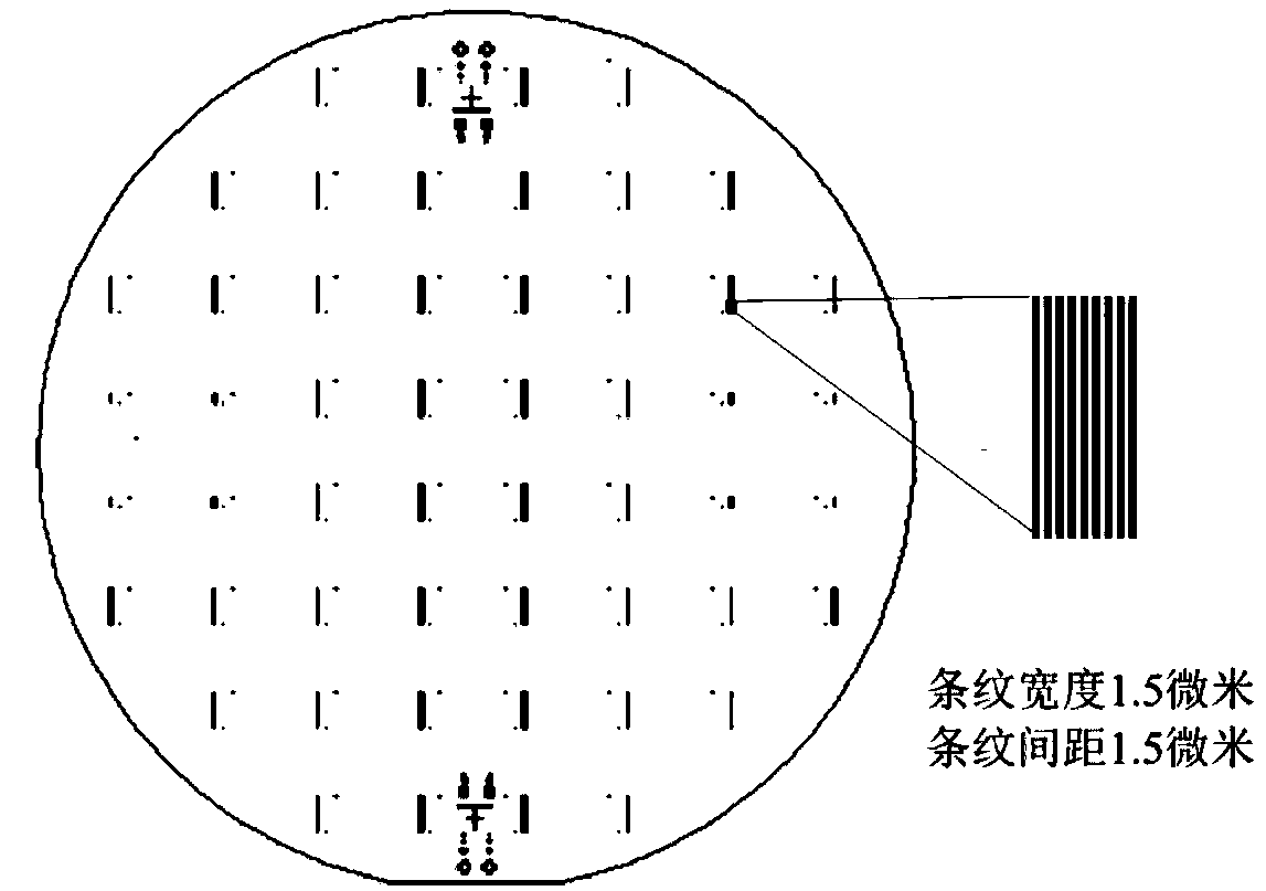
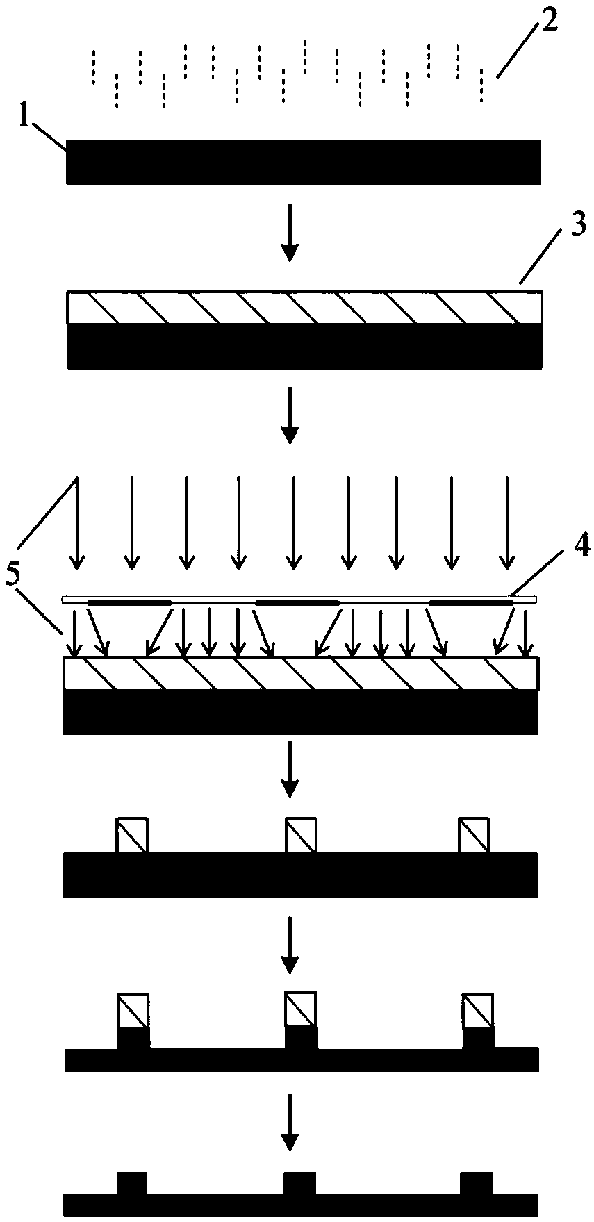
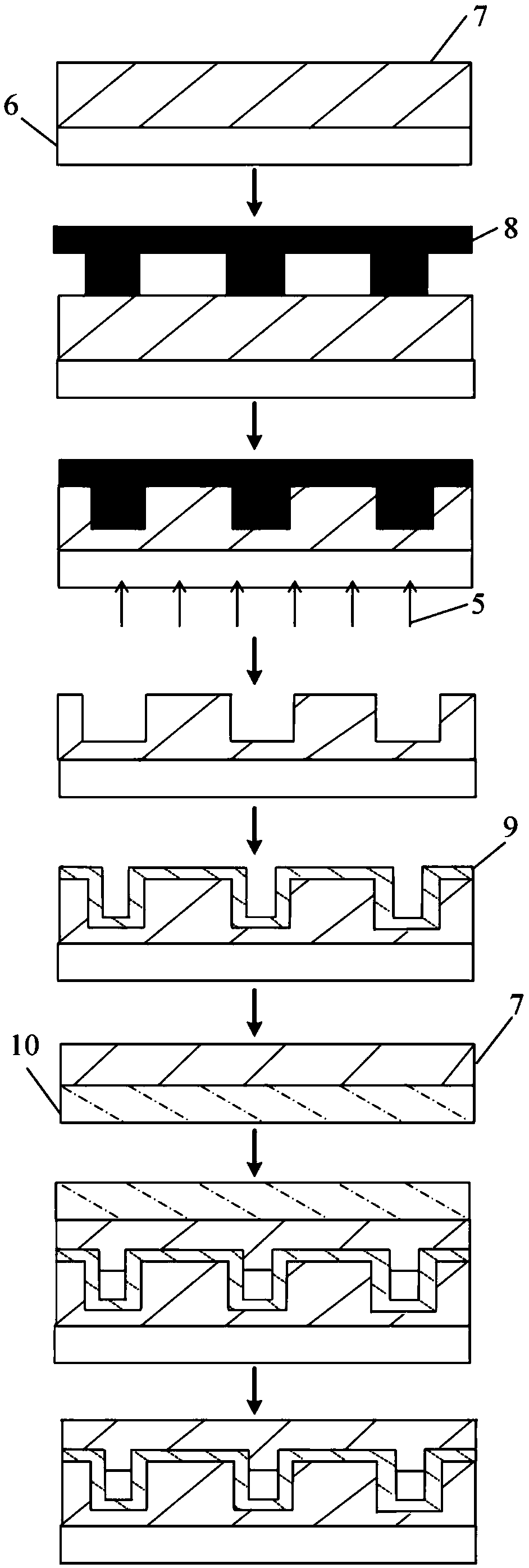
[0031] like figure 1As shown, the manufacturing process steps of the silicon nano-mold are as follows:

[0032] (a) Pour a small amount of hexamethyldisiloxane (HMDS) into the drying tower, let it stand for 10 minutes, make the drying tower full of HMDS2 steam, and then place the cleaned 4-inch silicon wafer 1 in the drying tower Treat for 20 minutes, take it out and preheat it on a hot plate for 3 minutes, so that a layer of adhesive layer is formed on the surface of the silicon wafer 1, and the bonding force between the silicon wafer 1 and the AZ703 photoresist 3 is improved.

[0033] (b) Spin-coat positive AZ703 photoresist 3 on the surface-modified silicon wafer 1 at a low speed of 600r / s for 9s, and at a high speed of 7000r / s for 30s. Pre-bake on a hot plate at 85° C. for 30 minutes to remove the solve...


PUM

PropertyMeasurementUnit
Sizeaaaaaaaaaa

Abstract

The invention belongs to the field of micro electromechanical system research, and relates to an approximate ultraviolet exposure and thin film growth method-based method for preparing a nanometer passage. An approximate ultraviolet exposure technology and a reaction ion etching technology are employed, a silicon nanometer die is fabricated, a pattern of the silicon nanometer die is transferred toa SU-8 photoresist die by hot stamping to form a nanometer channel, the channel size is reduced by growing a Parylene thin film to obtain a nanometer channel with a width smaller than 50 nanometers,the package of the nanometer channel is achieved through oxygen plasma auxiliary thermal bonding by a SU-8 photoresist cover plate, and a nanometer passage of which the height and the width both are smaller than 50 nanometers is finally obtained. The method has the characteristics of low cost and high production efficiency and is simple to operate.

Description

technical field [0001] The invention belongs to the field of micro-electromechanical research, and relates to a method for preparing nanometer channels based on proximity ultraviolet exposure and film growth methods. Background technique [0002] With the development of micro-nano technology, nanostructures have been widely used in the fields of biology, chemistry and electronics. Among them, nanochannel is a nanostructure with great application value, and its channel size is close to the size of biological macromolecules. There are irreplaceable advantages in studying biomolecules at the single-molecule level. [0003] At present, the manufacture of nanochannels mainly relies on equipment with nanoscale resolution, such as electron beam lithography, focused ion beam, and proton beam direct writing, etc., but its disadvantages are expensive equipment and high production costs, which are not conducive to mass production. In recent years, some researchers have used special pr...

Claims


Application Information

Patent Timeline
IPC IPC(8): G03F7/20G03F7/00B82Y40/00
CPCB82Y40/00G03F7/0002G03F7/2004
Inventor 邹赫麟孙蕾
Owner DALIAN UNIV OF TECH
Why Eureka
Try Eureka