A Fabrication Method of Surface Enhanced Raman Scattering Substrate Based on Aluminum Nitride Nanostructure

A surface-enhanced Raman and nanostructure technology, applied in the field of nanomaterials, can solve the problems of unfavorable mass production of disposable SERS substrates, small longitudinal depth of nanostructures on the substrate surface, cumbersome preparation process, etc., to reduce detection costs, The effect of low cost and high process repeatability

Active Publication Date: 2021-06-22
SHANDONG UNIV OF SCI & TECH
View PDF8 Cites 0 Cited by
  • Summary
  • Abstract
  • Description
  • Claims
  • Application Information

AI Technical Summary

Problems solved by technology

[0007] However, the main disadvantages of the above technical solutions are: (1) the longitudinal depth of the nanostructure on the surface of the substrate is small, which is not conducive to the adsorption of more substances to be tested; (2) the preparation process is cumbersome, and the silicon substrate and anodized aluminum template used Or the high cost of plasma dry etching is not conducive to mass production of disposable SERS substrates

Method used


Image

  • A Fabrication Method of Surface Enhanced Raman Scattering Substrate Based on Aluminum Nitride Nanostructure
  • A Fabrication Method of Surface Enhanced Raman Scattering Substrate Based on Aluminum Nitride Nanostructure
  • A Fabrication Method of Surface Enhanced Raman Scattering Substrate Based on Aluminum Nitride Nanostructure

Examples


Embodiment 1

[0043] A method for manufacturing a surface-enhanced Raman scattering substrate based on aluminum nitride nanostructures, comprising the following steps:

[0044] (1) Prepare the glass substrate and clean and dry it;

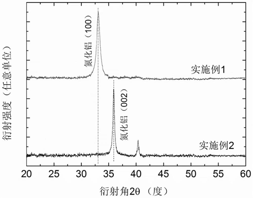
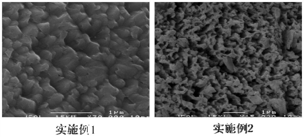
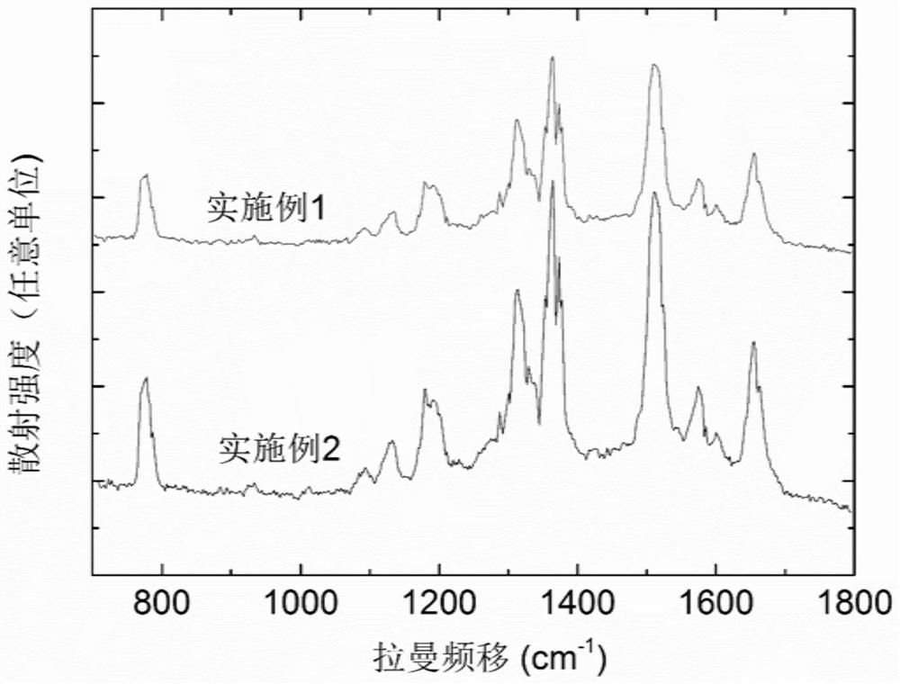
[0045] The aluminum nitride film with (100) texture is prepared on the substrate by magnetron sputtering method, the thickness is 100nm, and the process flow is as follows:

[0046] (i) Magnetron sputtering background vacuum pumped to less than 10 -3 Pa.

[0047] (ii) Applying a reverse bias voltage to perform plasma bombardment cleaning on the surface of the glass substrate to increase the binding force with the aluminum nitride film.

[0048] (iii) Use a high-purity aluminum target for reactive sputtering in a mixed atmosphere of nitrogen and argon. The preferred process parameters are: the volume ratio of nitrogen and argon is 7:3, the pressure of the sputtering atmosphere is 5Pa, and the sputtering power density is 4W / cm 2 .

[0049] (iv) After the spu...

Embodiment 2

[0057] A method for manufacturing a surface-enhanced Raman scattering substrate based on aluminum nitride nanostructures, comprising the following steps:

[0058] (1) Prepare the glass substrate and clean and dry it;

[0059] The aluminum nitride film with (002) texture is prepared on the substrate by magnetron sputtering method, the thickness is 200nm, and the process flow is as follows:

[0060] (i) Magnetron sputtering background vacuum pumped to less than 10 -3 Pa.

[0061] (ii) Applying a reverse bias voltage to perform plasma bombardment cleaning on the surface of the glass substrate.

[0062] (iii) Sputtering deposited tungsten metal with a thickness of 100 nanometers as a lattice mismatch buffer layer between (002) textured aluminum nitride and glass;

[0063] Use high-purity aluminum targets for reactive sputtering in a mixed atmosphere of nitrogen and argon, the volume ratio of nitrogen and argon is 2:8, the pressure of the sputtering atmosphere is 0.5Pa, and the ...


PUM

PropertyMeasurementUnit
thicknessaaaaaaaaaa
thicknessaaaaaaaaaa
thicknessaaaaaaaaaa

Abstract

The invention relates to a method for manufacturing a surface-enhanced Raman scattering substrate based on an aluminum nitride nanostructure, comprising the following steps: (1) preparing a (100) or (002) textured aluminum nitride film on a substrate; ( 2) using a strong alkali solution to etch the aluminum nitride film to obtain an aluminum nitride nanostructure; (3) using a mixture of concentrated nitric acid and hydrogen peroxide to hydroxylate the surface of the aluminum nitride nanostructure; (4) using a decompression The method of vapor deposition of aminopropyltriethoxysilane is used to modify amino groups on the surface of hydroxylated aluminum nitride nanostructures to obtain amino-modified aluminum nitride nanostructures; (5) assembling gold nanoparticles to amino-modified nitrogen Aluminum nanostructured surface, namely. The invention adopts the aluminum nitride film of sufficient thickness to form a nanostructure, which has a large adsorption surface area, can gather more molecules to be measured, and improves the intensity of Raman scattering, and the nanostructure can be controlled by etching conditions to obtain a controllable Raman enhancement effect.

Description

technical field [0001] The invention relates to the technical field of nanometer materials, in particular to a method for manufacturing a surface-enhanced Raman scattering substrate. Background technique [0002] Surface-Enhanced Raman Scattering (SERS) spectroscopy is a trace analysis technique with great application potential in the fields of electrochemistry, environmental analysis and biomedicine. By constructing a rough metal surface, the adsorbed compound is excited by the surface localized plasmons to cause electromagnetic enhancement, and the atomic clusters and adsorbed molecules on the rough surface form Raman-enhanced active sites. Raman scattering greatly enhances the spectral intensity. SERS technology has the advantages of selectivity and ultra-sensitivity of fingerprinting. The key issue to realize the wide application of this technology is to prepare SERS substrates with extremely high Raman enhancement ability, spectral reproducibility and large-area unifo...

Claims


Application Information

Patent Timeline
Patent Type & Authority Patents(China)
IPC IPC(8): G01N21/65
CPCG01N21/658
Inventor 陈达王鸿飞王璟璟王鹏
Owner SHANDONG UNIV OF SCI & TECH
Why Eureka
Try Eureka