Two-dimensional material field effect transistor with transverse structure, and preparation method and application thereof

A technology of field effect transistors and two-dimensional materials, which is applied in semiconductor/solid-state device manufacturing, semiconductor devices, electrical components, etc., can solve problems affecting the electrical performance of two-dimensional material field effect transistors, reduce contact barriers, and improve electrical properties. performance, easy operation

Inactive Publication Date: 2018-11-23
GUANGDONG UNIV OF TECH
View PDF4 Cites 5 Cited by
  • Summary
  • Abstract
  • Description
  • Claims
  • Application Information

AI Technical Summary

Problems solved by technology

However, due to the influence of the Fermi level pinning effect and the difficulty of heavy doping in two-dimensional materials, there is often a Schottky barrier in the contact between two-dimensional materials and metal electrodes, which affects the two-dimensional materials to some extent. Electrical Properties of Field Effect Transistors

Method used


Image

  • Two-dimensional material field effect transistor with transverse structure, and preparation method and application thereof
  • Two-dimensional material field effect transistor with transverse structure, and preparation method and application thereof

Examples


Embodiment 1

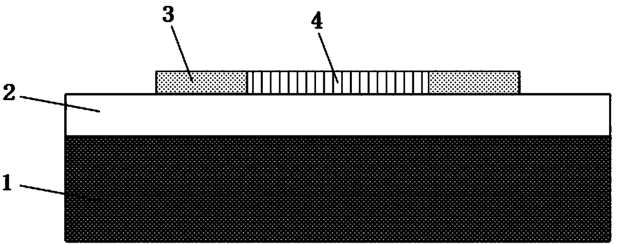
[0025] A two-dimensional material field effect transistor with a lateral structure. From bottom to top, there are substrate silicon 1, dielectric layer hafnium dioxide 2, metal electrode titanium 3, and two-dimensional material titanium disulfide 4, such as figure 1 Shown. The two-dimensional material titanium disulfide is formed in the middle part of the metal titanium by the sulfidation method, and a covalent bond is formed between the two-dimensional material titanium disulfide and the metal electrode titanium, effectively forming an ohmic contact.

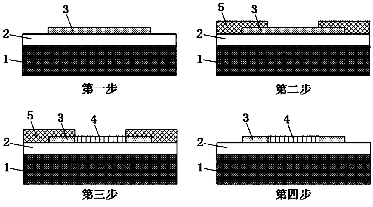
[0026] The manufacturing method of the above-mentioned two-dimensional material field effect transistor with lateral structure, such as figure 2 As shown, including the following steps:

[0027] In the first step, the dielectric layer 2 is plated on the substrate 1 by chemical vapor deposition, and then a layer of metal 3 is plated on the dielectric layer 2 by electron beam evaporation; the material of the substrate 1 is silicon, a...

Embodiment 2

[0032] A two-dimensional material field-effect transistor with a lateral structure. From bottom to top, there are substrate germanium 1, dielectric layer zirconium dioxide 2, metal electrode molybdenum 3, two-dimensional material molybdenum diselenide 4, such as figure 1 Shown. The two-dimensional material molybdenum diselenide is formed in the middle part of the metal molybdenum by the selenization method, and a covalent bond is formed between the two-dimensional material molybdenum diselenide and the metal electrode molybdenum, effectively forming an ohmic contact.

[0033] The manufacturing method of the above-mentioned two-dimensional material field effect transistor with lateral structure, such as figure 2 As shown, including the following steps:

[0034] In the first step, a layer of metal 3 is plated on the dielectric layer 2 by chemical vapor deposition on the substrate 1. The material of the substrate 1 is germanium, the material of the dielectric layer 2 is zirconium dio...

Embodiment 3

[0039] A two-dimensional material field-effect transistor with a lateral structure. From bottom to top, there are substrate germanium 1, dielectric layer zirconium dioxide 2, metal electrode molybdenum 3, two-dimensional material tungsten diselenide 4, such as figure 1 Shown. A two-dimensional material tungsten diselenide is formed in the middle part of the metal tungsten by the selenization method, and a covalent bond is formed between the two-dimensional material tungsten diselenide and the metal electrode tungsten, effectively forming an ohmic contact.

[0040] The manufacturing method of the above-mentioned two-dimensional material field effect transistor with lateral structure, such as figure 2 As shown, including the following steps:

[0041] In the first step, a layer of metal 3 is plated on the substrate 1 using a chemical vapor deposition method to plate the dielectric layer 2; wherein the material used for the substrate 1 is germanium, the material used for the dielectri...


PUM

PropertyMeasurementUnit
thicknessaaaaaaaaaa
thicknessaaaaaaaaaa
thicknessaaaaaaaaaa

Abstract

The invention belongs to the technical field of micro-nano electronics, and discloses a two-dimensional material field effect transistor with a transverse structure, and a preparation method and an application thereof; the two-dimensional material field effect transistor sequentially comprises a substrate, a dielectric layer, a metal electrode and a two-dimensional material from bottom to top, wherein the two-dimensional material is a metal sulfide or a metal selenide; the middle part of the metal is made to form the two-dimensional material through a vulcanization method or a selenization method, so that covalent bonds are formed between the two-dimensional material and the metal electrode, and ohmic contact is effectively formed. The preparation method of the transverse structure two-dimensional material field effect transistor has the advantages of simplicity in operation, few process steps and high efficiency, ohmic contact is effectively formed, the contact barrier between the two-dimensional material and the metal electrode is reduced, and the electrical property of the device is improved.

Description

Technical field [0001] The invention belongs to the technical field of micro-nano electronics, and more specifically, relates to a two-dimensional material field effect transistor with a lateral structure and a preparation method and application thereof. Background technique [0002] Since the appearance of two-dimensional materials represented by graphene, it has attracted a lot of attention and research due to its distinctive electrical, optical, magnetic and mechanical properties. As a supplement to graphene, two-dimensional transition metal chalcogenides often have a certain band gap and unique mechanical, optical, electrical and other physical properties, and have gradually become an emerging two-dimensional material system. Research on two-dimensional material field effect transistors is also increasing. Flourish. However, due to the Fermi level pinning effect and the difficulty of heavy doping of two-dimensional materials, there is often a Schottky barrier in the contact ...

Claims


Application Information

Patent Timeline
Patent Type & Authority Applications(China)
IPC IPC(8): H01L29/417H01L29/423H01L29/45H01L29/78H01L21/34H01L21/44
CPCH01L29/401H01L29/41725H01L29/4232H01L29/45H01L29/66969H01L29/78
Inventor 杨亿斌李京波招瑜肖也罗东向牟中飞郑照强
Owner GUANGDONG UNIV OF TECH
Why Eureka
Try Eureka