

A kind of integrated SBD silicon carbide trench mosfets and its preparation method
A technology of silicon carbide trench and silicon carbide substrate, which is applied to the structure and preparation of trench metal-oxide-semiconductor field effect transistors, and can solve the problem of excessive electric field
- Summary
- Abstract
- Description
- Claims
- Application Information
AI Technical Summary
Problems solved by technology
Method used
Image

Examples
preparation example Construction
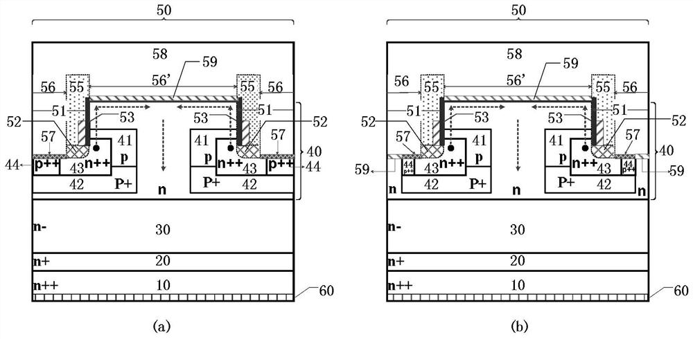
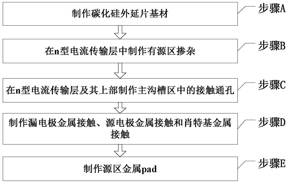
[0109] figure 2 It is a schematic diagram of the steps of the preparation method, such as figure 2 Shown, described preparation method comprises:
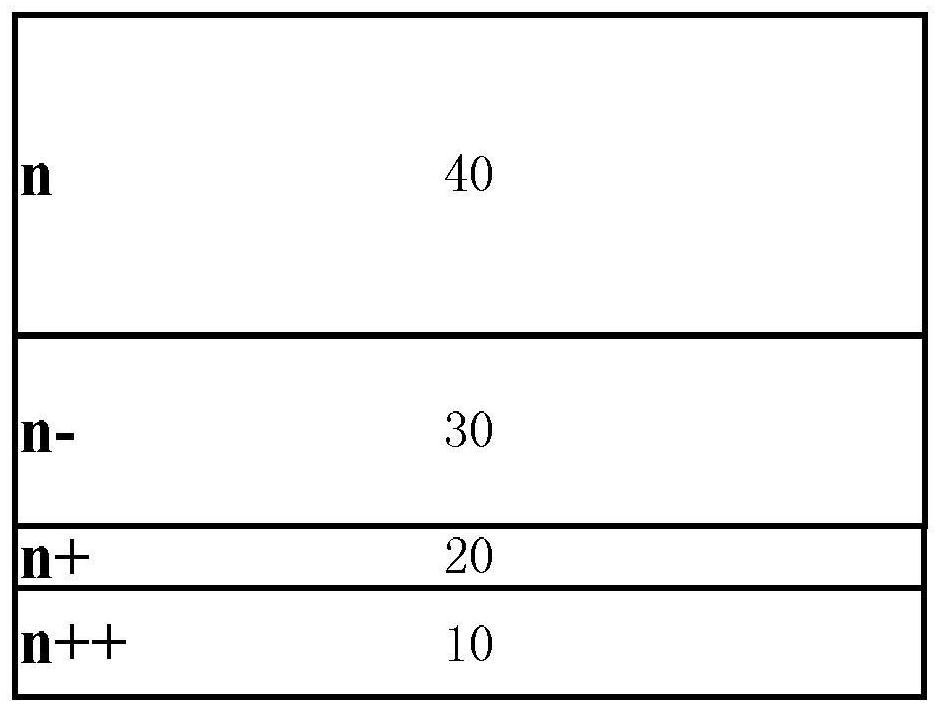
[0110] Step A: making a silicon carbide epitaxial wafer substrate; including, sequentially growing an n+ type buffer layer 20, an n-drift layer 30 and an n-type current transport layer 40 on an n++ type silicon carbide substrate 10 from bottom to top, as image 3 shown;
[0111] Step B: Doping the active region in the n-type current transport layer 40, including:
[0112] method 1)
[0113] Sub-step B1: Deposit an implantation mask on the n-type current transport layer 40, pattern it by photolithography, and use doping methods such as ion implantation to form a top-down p-type trench in the n-type current transport layer 40 channel layer 41 and p+ type shielding layer 42, such as Figure 4 shown;
[0114] In the sub-step B1, the doping concentration range of the p-type channel layer 41 is 1×10 16 cm -3 ~1×10 18 cm -3 , ...
PUM
| Property | Measurement | Unit |
|---|---|---|
| thickness | aaaaa | aaaaa |
Abstract
Description
Claims
Application Information