
A method for improving the field emission performance of graphene sheet-carbon nanotube array composites

A carbon nanotube array and graphene sheet technology, which is applied in the preparation and application of nanomaterials, can solve the problems of large number of field emission points, poor stability, and low work function, and achieve the goal of increasing the maximum field emission current density, The effect of promoting the transport of electrons and reducing the work function

Inactive Publication Date: 2019-12-31
TIANJIN NORMAL UNIVERSITY
View PDF9 Cites 0 Cited by
  • Summary
  • Abstract
  • Description
  • Claims
  • Application Information

AI Technical Summary

Problems solved by technology

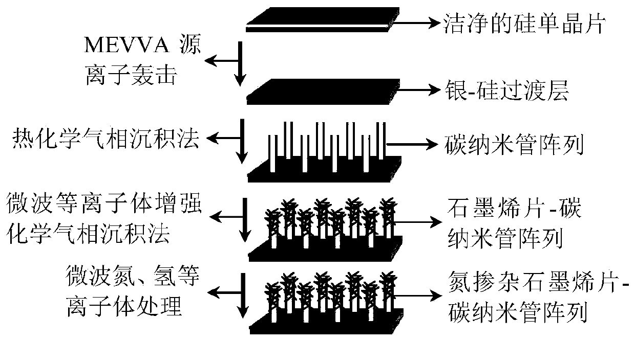
[0003] The purpose of the present invention is to overcome the shortcomings of the existing graphene sheet-carbon nanotube array-based field emission cathode operating electric field is relatively high, the field emission current density is small, and the stability is not good during high current density field emission, The transition layer was introduced by silver ion bombardment to strengthen the bonding force between carbon nanotubes and silicon single wafer, and nitrogen-doped graphene sheet-carbon with low work function and large number of field emission points was obtained by microwave nitrogen and hydrogen plasma treatment. Nanotube array composite material, and finally obtain a field emission cathode composite material with low working electric field, large field emission current density and good field emission stability under high current density

Method used


Image

  • A method for improving the field emission performance of graphene sheet-carbon nanotube array composites
  • A method for improving the field emission performance of graphene sheet-carbon nanotube array composites
  • A method for improving the field emission performance of graphene sheet-carbon nanotube array composites

Examples


Embodiment 1

[0027] (1) Pretreatment of silicon single wafer:

[0028] First cut the silicon single wafer into small pieces of 2cm×2cm, then ultrasonically (50W) clean them in deionized water and absolute ethanol for 5 minutes, and then immerse the silicon single wafer in 4% hydrofluoric acid by volume After 5 minutes, take it out and dry it, then carry out energy-carrying silver ion bombardment pretreatment in the silicon single wafer with clean surface obtained in a metal vapor vacuum arc ion source (MEVVA source), and keep the sample stage rotating at a constant speed during the bombardment , the sample stage bias voltage was set to -15kV, the beam current was 10 mA, and the bombardment time was 10 minutes.

[0029] (2) Preparation of carbon nanotube arrays by thermal chemical vapor deposition and high temperature annealing treatment:

[0030] Put the silicon single wafer that step (1) obtains into the magnetron sputtering device and deposit the iron catalyst film with a thickness of 5...

Embodiment 2

[0038] (1) Pretreatment of silicon single wafer:

[0039] First cut the silicon single wafer into small pieces of 2cm×2cm, then ultrasonically (50W) clean them in deionized water and absolute ethanol for 5 minutes, and then immerse the silicon single wafer in 4% hydrofluoric acid by volume After 5 minutes, take it out and dry it, then carry out energy-carrying silver ion bombardment pretreatment in the silicon single wafer with clean surface obtained in a metal vapor vacuum arc ion source (MEVVA source), and keep the sample stage rotating at a constant speed during the bombardment , the sample stage bias voltage was set to -15kV, the beam current was 10 mA, and the bombardment time was 10 minutes.

[0040] (2) Preparation of carbon nanotube arrays by thermal chemical vapor deposition and high temperature annealing treatment:

[0041] Put the silicon single wafer that step (1) obtains into the magnetron sputtering device and deposit the iron catalyst film with a thickness of 5...

Embodiment 3

[0049] (1) Pretreatment of silicon single wafer:

[0050] First cut the silicon single wafer into small pieces of 2cm×2cm, then ultrasonically (50W) clean them in deionized water and absolute ethanol for 5 minutes, and then immerse the silicon single wafer in 4% hydrofluoric acid by volume After 5 minutes, take it out and dry it, then carry out energy-carrying silver ion bombardment pretreatment in the silicon single wafer with clean surface obtained in a metal vapor vacuum arc ion source (MEVVA source), and keep the sample stage rotating at a constant speed during the bombardment , the sample stage bias voltage was set to -15kV, the beam current was 10 mA, and the bombardment time was 10 minutes.

[0051] (2) Preparation of carbon nanotube arrays by thermal chemical vapor deposition and high temperature annealing treatment:

[0052] Put the silicon single wafer that step (1) obtains into the magnetron sputtering device and deposit the iron catalyst film with a thickness of 5 n...


PUM

PropertyMeasurementUnit
current densityaaaaaaaaaa

Abstract

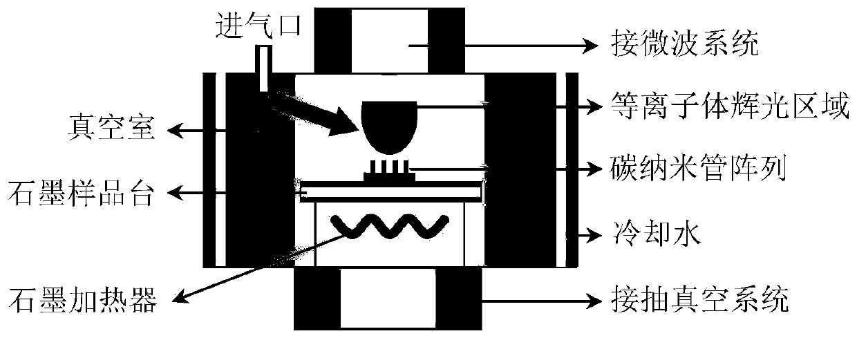
The invention discloses a method of improving field emission performance of the graphene sheet-carbon nanotube array composite material belongs to the field of preparation and application of nanomaterials. Includes such steps as pre-treating silicon single crystal wafer by silver ion bombardment, preparing silicon single crystal wafer by silver ion bombardment, preparing silicon single crystal wafer by silver ion bombardment, (2) preparing carbon nanotube by thermochemical vapor deposition and annealing at high temperature; 3) preparing thin-layer graphene sheets on the carbon nanotube array by microwave plasma enhance chemical vapor deposition method; (4) obtaining graphene sheet- Carbon nanotube arrays were treated by nitrogen and hydrogen plasma at room temperature. Compared with the prior art, the nitrogen-doped graphene sheet prepared by the method has the advantages that: the Carbon nanotube array composites have very low working electric field, very high current density and goodfield emission stability under high current density, so they have very high application value.

Description

technical field [0001] The invention belongs to the technical field of preparation and application of nanomaterials, and in particular relates to a method for preparing a nitrogen-doped graphene sheet-carbon nanotube array composite material by plasma treatment and for improving field emission performance. Background technique [0002] Field emission refers to the process of electrons inside the cathode material escaping from the surface of the material into the vacuum under the action of an externally enhanced electric field. Excellent field emission performance generally requires the cathode to have a low working electric field, a large current density and good stability. sex. As a quasi-one-dimensional nanomaterial, carbon nanotubes have a large aspect ratio and excellent electrical conductivity, making them an ideal field emission cathode material. The preparation of vacuum field electronic devices such as displays has shown good application prospects. However, when pu...

Claims


Application Information

Patent Timeline
Patent Type & Authority Patents(China)
IPC IPC(8): H01J1/304H01J9/02B82Y30/00B82Y40/00
CPCB82Y30/00B82Y40/00H01J1/304H01J9/025
Inventor 邓建华朱文祥张燕
Owner TIANJIN NORMAL UNIVERSITY
Learn More